
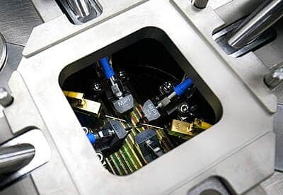
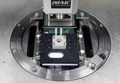
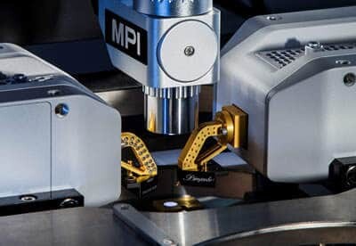
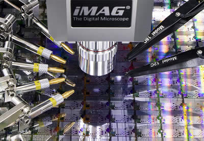
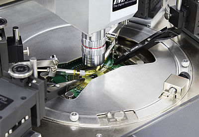
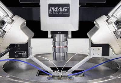
MPI Laser Cutter System LCS-635
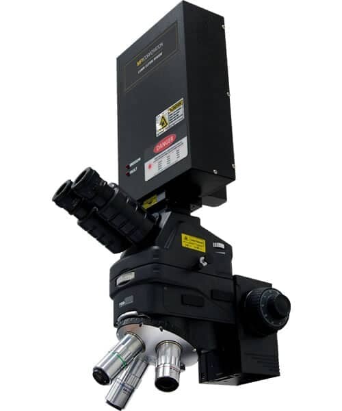
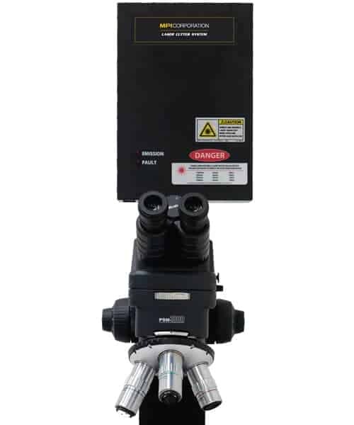
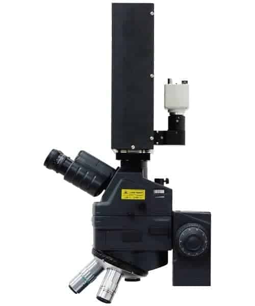
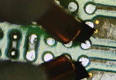
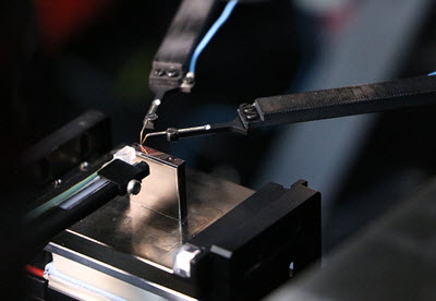
The unique MPI Laser Cutter System LCS-635 is designed for accurate and reliable Failure Analysis and Design Validation applications. Variable configurations based on 1064 nm, 532 nm, 355 nm or 266 nm wavelengths provides the capability to remove several semiconductor materials and metals selectively, see below the table.
