
Silicon Photonics On-Wafer Test

MPI Definition
The requirement to increase bandwidth in all phases of wire and/or wireless communications combined with an increase in data center speed is driving the communication world away from copper interconnects and towards Silicon Photonics. This evolving technology uses a combination of fiber optics, optical wave guides, integrated optics, optical amplifiers, laser frequency light waves, and photo detectors to carry far more data than traditional copper conductors, to support faster data transfer rates between data communication centers.
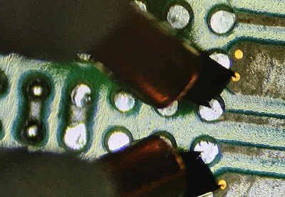
There are many new processes and capabilities which require to perform variety of non-conventional on-wafer measurements, such as pure parametric optical: Insertion Loss (IL), polarization dependent loss (PDL) measurements, Optical/Electrical S-Parameters, E-E, E-O, O-E, O-O, optical eye, jitter, transmitter and dispersion eye closure (TDEC), and e.g. on the receiver side bit-error-rate (BER) testing.
Major Requirements
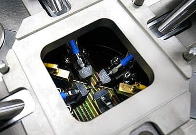
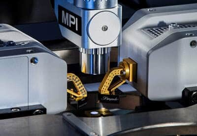
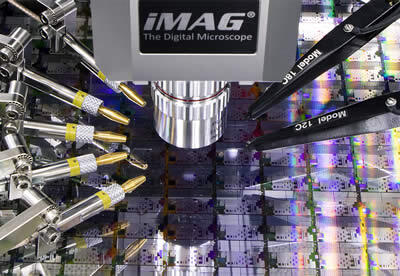
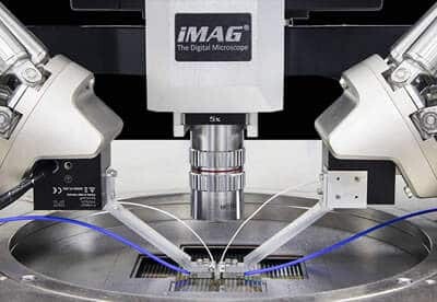
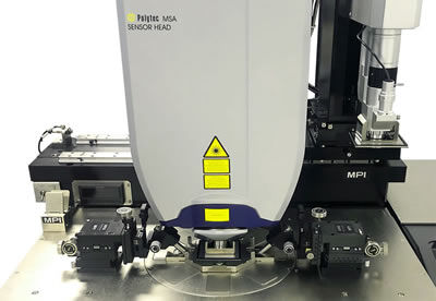
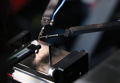
Integration of very accurate single and/or multi-fiber array alignment systems, in combination with common electrical DC and RF signals. Probe arms with optical fiber matching the device operating wavelength and gradient coupler’s angles.
Automated and highly precise Z-sensing for keeping the fibers in constant few micrometer distance to the optical I/Os. High mechanical stability and vibration isolation control in order to minimize e.g. trans-impedance amplifier (TIA) output voltage variations.
MPI Solutions
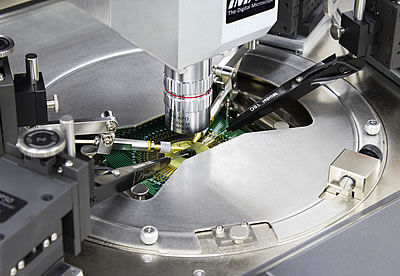
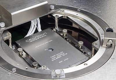
MPI designed dedicated SiPH probe systems for silicon photonics on-wafer tests. The systems are designed with a reduced platen to chuck distance which allows shorter overall fiber length for performing repeatable low noise measurements.
Variety of accurate up to 6-axis fiber positioning stages and related software can be easily configured with the MPI SiPH probe systems in order to meet different requirements. Easy upgrade path safes budgets and time, if requirements are changing.
Solutions for just single fiber or multi-fiber-arrays are available, all integrated with automated Z-sensing unit for constant distance of few micrometer to the optical I/O. MPI provides unique safety concept offering of an integrated crash protection to prevent not only collisions of the wafer to the fiber at initial set-up but also of both independent I/O fibers/arms.
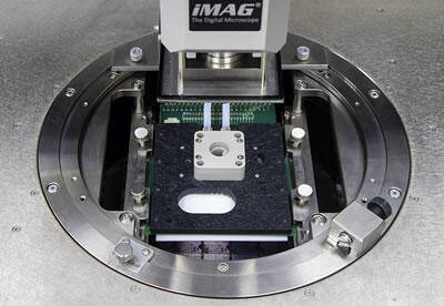
Seamless integrated measurement rack accommodates controllers, drivers very close and convenient to operate by not consume additional floor space.