
MPI PCB Probe Systems – Comprehensive Manual Probing Solutions

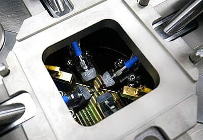
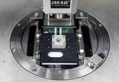
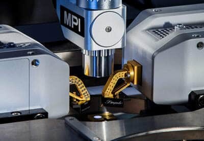
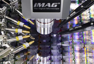
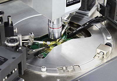
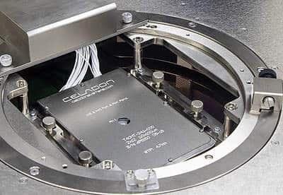
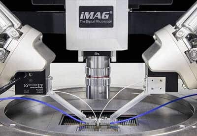
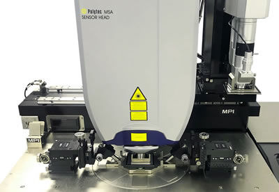
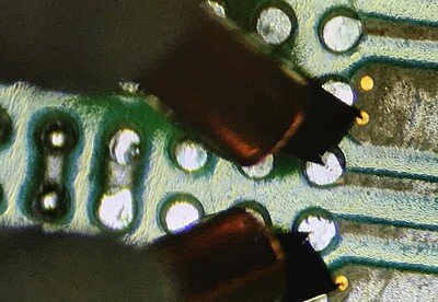
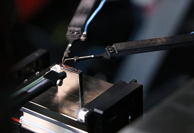
Experience unparalleled versatility with every MPI manual probe systems , designed to accommodate a wide range of printed circuit board (PCB) holders for convenient and accurate Signal Integrity (SI) measurements. Our systems enable single-ended or differential RF probe measurements for eye-patterns, deterministic jitter, distortion, TDR impedance, cross-talk, coupling, losses, and S-parameters.
Our TS150-THZ & TS200-THZ systems offer an extended frequency range up to sub-THz, making them the most versatile manual probe stations available on the market. These systems are suitable for various applications, including research and development, quality assurance, and production testing, ensuring accurate and reliable measurements across a wide frequency range.
MPI PCB Probe Systems
TS300-PCB

TS600-PCB
