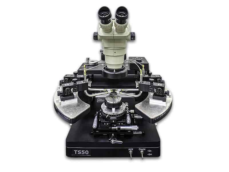
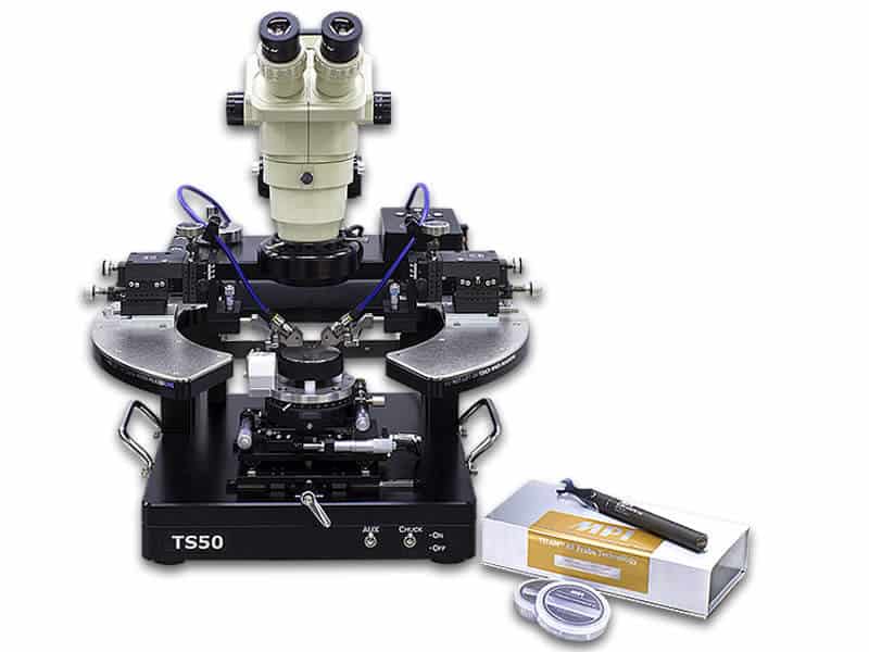
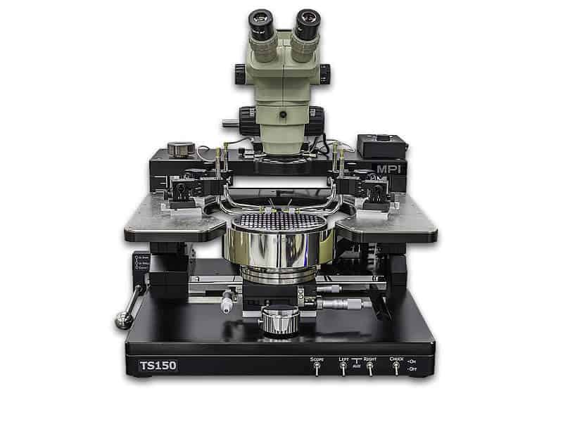
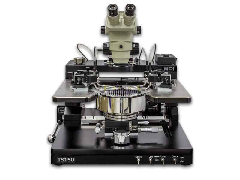
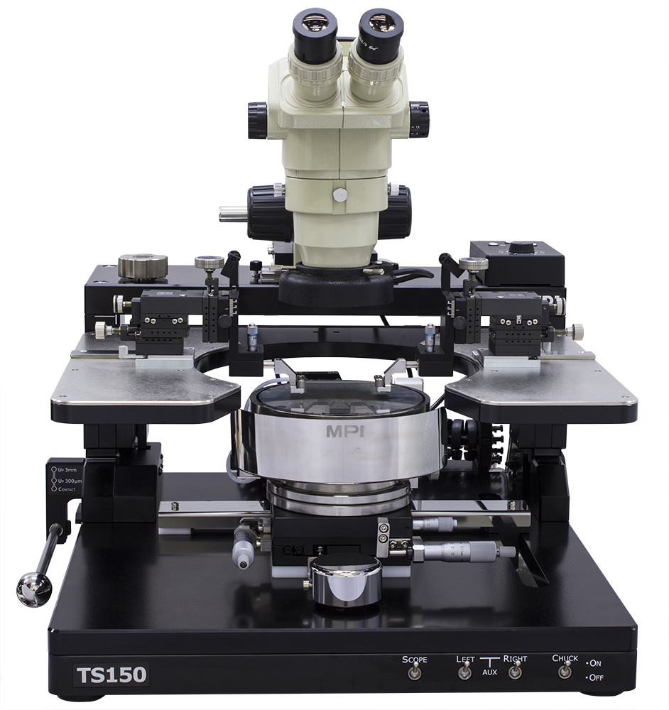
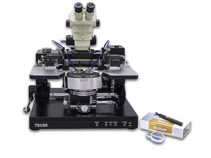
MPI IMPACT™ Test Solutions for Education

Tailored Solutions

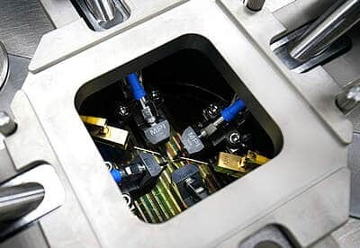
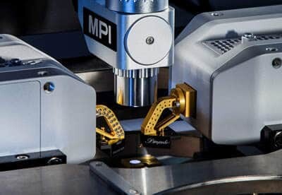
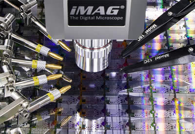
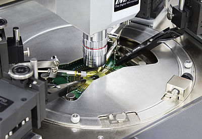
IMPACT™ Test Solutions (ITS) are complete and flexible packages – unlike “pre-defined packages” – IMPACT is well tailored to all applications and individual requirements.  Achieved without compromising quality or measurement accuracy.

Wafer Test Solution

Features

Cost-effective, however without compromising the quality of the user experience by convenient and accurate operation.

Therefore, ALL MPI systems are configured with:

  • XY linear microscope movement on stable bridge
  • Probe platen with fine Z-adjustment and/or platen lift
  • XY chuck stages with accurate down to one micrometer positioning
  • Fine THETA chuck control with micrometer precision
  • 150 mm systems with MPI unique air-bearing stage
MPI IMPACT™ Package - ITS25-THZ
MPI IMPACT™ Package - ITS150-THZ

Example

If the application requires measuring RF signals at a lower frequency range – the right choice would be the ITS150-RF26. Should the measurement frequency be higher, select the 40 GHz, 50 GHz, or even the 67 GHz option.

These configurations can grow and the price will simply adjust to the difference between the cables and the RF probes themselves. 

In the end the final configuration is a true reflection of the requirement at a corresponding price.

Complete Test Solution

With IMPACT™, MPI is providing a significant impact to the Cost of Test by offering very attractive pricing, an easy upgrade path, and a wide variety of interchangeable options.  IMPACT™ addresses the specific requirements of universities, public, government institutes, and research centers in DC/CV or RF applications.

Wafer Test Solution

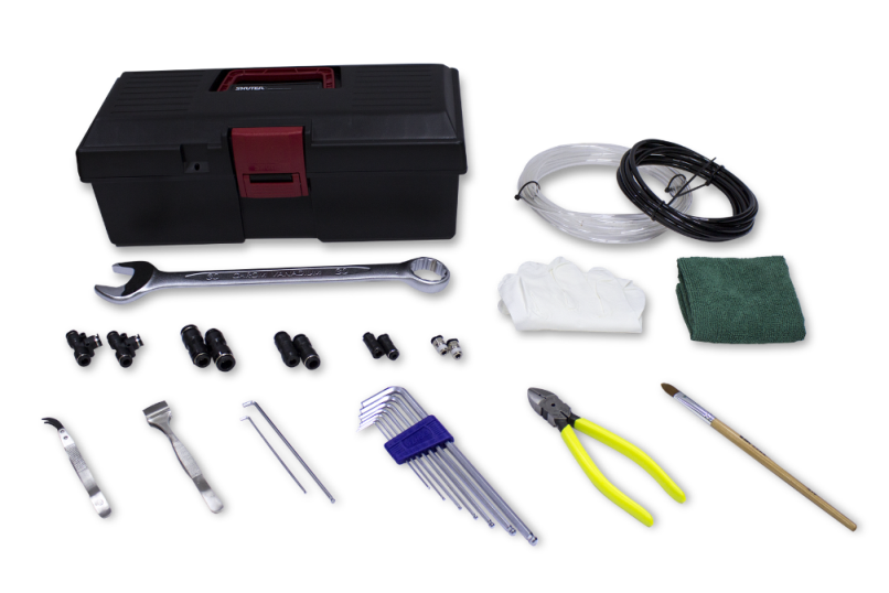
What else is inside?

With the simplicity of a single part number, all MPI ITS packages include:

  • An extended warranty
  • Installation instructions and all associated tools
  • Free shipment worldwide
  • Free registration of MPI’s new and revolutionary QAlibria® RF calibration software*
  • Free local application support by phone or email

* in case of RF packages

MPI is listening and understands customer demands and MPI is turning that understanding into value based products – faster than ever before! 

Field Application Engineer

Job Location: San Jose, CA

Job Duties:

  • Assist in developing HW and SW measurement methodologies/solutions for analytical wafer probe solutions with signal applications from DC to millimeter wave frequencies as well as Silicon Photonics (SiPH);
  • Collaborate with customers on their measurement challenges, and provide applications specific product training;
  • Provide pre- and post-sale support to AST, customers, service department, and the sales channel developing HW and SW measurement solutions for analytical wafer probe stations;
  • Define application-specific solutions based on customer-provided device data and facilitate both customer and divisional teams to successful results;
  • Perform product training seminars for customer and sales channels as well as participate in trade shows and technical seminars;
  • Make recommendations regarding product improvement, new products, and quality enhancement;
  • Author, document, publish, and present measurement solutions via Seminars, Applications Notes, Briefs, and White Papers;
  • Prepare, plan, and assist with customer product demonstrations that highlight value-based differentiation of AST product offerings;
  • Develop unique and individual customer presentations designed to professionally position the MPI brand in the North American market and deliver formal presentations to customers.

Job Requirements:

Master’s degree in Electrical Eng., Electronics Eng., Physics, or Photonics; Must possess 6 months of relevant work experience; Travel to customers’ sites in US and headquarters in Taiwan is required.

Send resume to: MPI America, Inc., 2360 Qume Drive, Suite C, San Jose, CA 95131, Attn: Janet Chiang