
High Power Device Tests

MPI Definition
Electrical measurements of high power discrete devices like power transistors, power diodes, thyristors etc.. designed in vertical and/or lateral device orientation, or even high power amplifiers.
Major Requirements
Measurement conditions required more than 500V (high voltage) and/or 1A (high current) in pulse or DC.
On-wafer characterization applications of high power devices face specific challenges such as:
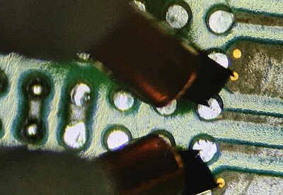
- Chuck to wafer backside contact resistance,
- High current device pad burnout, and
- Low leakage measurement at high voltage over temperature
- High voltage arcing,
- Thin-wafer handling and
- Safety test environment
- Chuck to wafer backside contact resistance,
- High current device pad burnout, and
- Low leakage measurement at high voltage over temperature
- High voltage arcing,
- Thin-wafer handling and
- Safety test environment
MPI Solutions
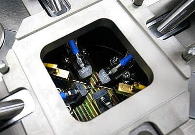
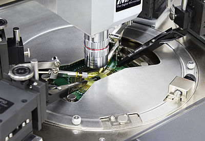
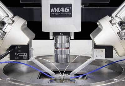
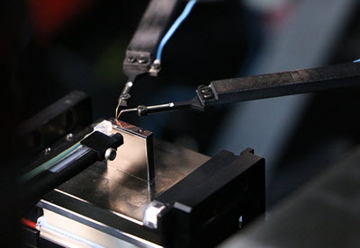
MPI’s High Power Probe Systems provide for accurate measurements of high power devices up to 3 kV (triaxial)/10 kV (coaxial) and 400 A (pulse) to include elevated temperatures of up to 300 °C. MPI’s gold plated high power thermal chucks, with evenly distributed vacuum holes located across the chuck, safely secure thin/warped wafers down to 50 µm. These high power chucks also provide excellent backside wafer contact while achieving low contact resistance for vertical device RDS(on) measurements.
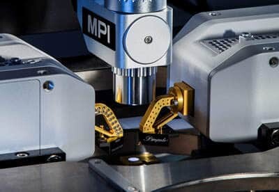
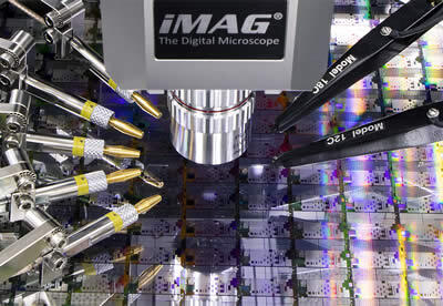
Multi contact High Current Probes (HCP) not only reduce the probe contact resistance but also avoid device pad burnout usually associated with single needle probes by distributing current. MPI’s high voltage probes (HVP) are designed to withstand up to 10 kV for low leakage device breakdown measurements. The UHP probes are combining both capabilities and eliminating the need to change probes for high voltage and current applications.
To suppress high voltage measurement arching, MPI solutions include specially design trays for Fluorinert™ liquid or dedicated anti-arcing probe card, which can be used uniquely even at higher temperature.
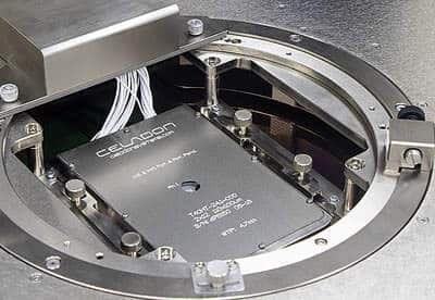
TAIKO wafer support is available on all MPI’s High Power Probe Systems, which are designed to integrate with various test instruments, such as Keithley or Keysight SMUs, and provide fast system setup for various device test conditions.
TS2500 is MPI’s 200 mm fully automatic probe system series, specifically developed to address High Power device testing at the production level. The system is designed for 24/7 production reliability and compatible with all MPI system accessories.
MPI high power probing solutions comes with safety systems and are tested for regulatory safety 3rd party certificates.
*Fluorinert is a trademark of 3M Company, USA.