
Device Characterization for Modeling and Process Development

MPI Definition
Semiconductor device modeling creates models for behavior of the discrete, elementary devices (transistors, inductors, diodes, etc.) based on fundamental physics, geometry, design and operation conditions.
One of the important steps is to perform very accurate electrical on-wafer measurements of such devices and this step is general known as Device Characterization.
Driven by emergence of the new device technologies, new materials, processes development and integration, the Device Characterization process faces increasing challenges in electrical test for more and more sophisticated devices and for higher amount of data extraction.
Major Requirements
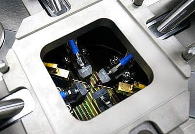
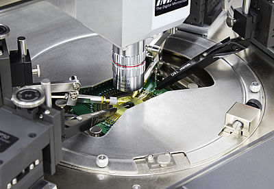
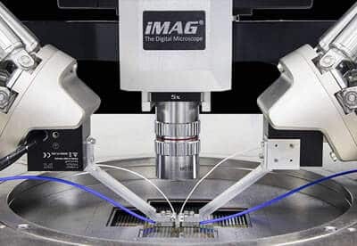
Basic device characterization and modeling requires accurate I-V/C-V, 1/f, RTN, RF, mmW, load pull and noise measurement of devices under temperature controlled and EMI-shielded test environment.
Typical technical challenges include repeatability of the measurement, reliable probe contact, internal or external noise influences, current leakage of the probes and chucks, thermal performance of the system, testing over a variety of temperatures, reducing the soaking time, and correct electrical connections between the device and various instruments.
The increased demand for more data extraction is leading into the necessary desire for more and more automation during the Device Characterization process. Therefore, in addition to all technical needs, reducing the overall cost-of-test by increasing the test cell efficiency and/or increasing the level of automation are key economic requirements.
MPI Solutions
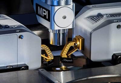
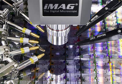
MPI Engineering Probe Systems are designed to provide accurate measurement results with maximum confidence. With the dedicated Accessories such as coaxial, Kelvin, triaxial measurements connection, thermal chucks with leakage performance down to fA level over the temperature range from -60 to 300 °C and superior thermal distribution, EMI-shielded and light-tight test environment, the MPI probe systems with ShielDEnvironment™ (TS200-SE, TS2000-SE, TS300-SE, TS3000-SE, and now TS3500-SE) are the heart of performing accurate Device Characterization.
Optimizing the test flow, shorting the soaking time with the new AirCool® PRIME thermal chucks, or even using hot/cold wafer swapping are typical MPI solutions for reducing the test time while increasing test-cell efficiency.
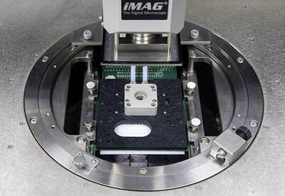
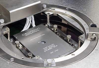
MPI’s WaferWallet® extends the TS3500-SE automation without compromising measurement capability. It is designed with five individual trays for manual, ergonomic loading of 150, 200, or 300 mm “modeling” wafers for fully-automated tests.
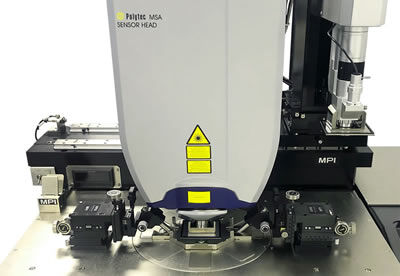
Complete RF measurement solutions for device modeling provides precision RF measurement results and calibrations up to 110 GHz by employing MPI’s calibration software QAlibria® and MPI RF Probes.