
Wafer Level Reliability (WLR)

MPI Definition
Reliability is defined as the ability of a device to conform to its electrical specifications over a specified period of time under specified conditions at a specified confidence level. Once an integrated circuit (IC) has been designed and the first silicon comes out, Wafer Level Reliability (WLR) tests are performed to accelerate new IC designs and processes verification by assessing the reliability characteristics portion of the technology process. Examples:
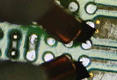
- Device Reliability: HCI, NBTI, PBTI…
- Gate Oxide Integrity: TDDB, V-Ramp. HV-GOI…
- Metal Interconnects: EM, ILD TDDB….
Major Requirements
The major challenge for WLR probing is to meet the contradictory requirements of the typical measure-stress-measure testing : high throughput, high flexibility, long-term measurements and sometimes at extreme temperatures.
MPI Solutions
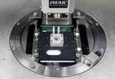
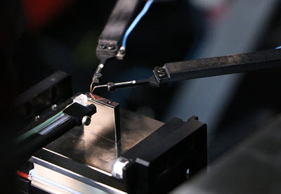
MPI 300 °C AirCool® PRIME thermal chucks provide excellent flatness over entire temperature range and therefore provide deliver unparalleled performance for multi-site testing. Faster transition time of a chuck is a desirable factor in short term reliability tests at multiple temperatures to enhance the productivity.
On the other hand, reliability of the thermal system which consists of chuck, controller and the chiller, the embedded active probe platen cooling and the ability of the probe systems to assure stable contact over time are essential for long term WLR testing and minimization of the overall cost of test.
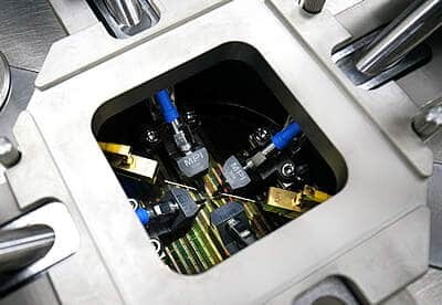
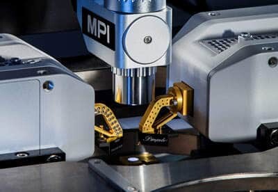
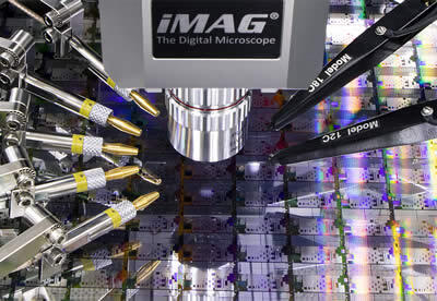
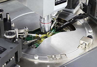
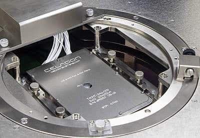
MPI integration of Celadon Systems high performance probe card inside MPI Automated Probe Systems like TS2000-SE or TS3000-SE, makes the high density, multi-site, high temperature wafer level reliability testing easy and versatile.
MPI’s WaferWallet® extends the TS3500-SE automation significantly without compromising measurement capability. It is designed with five individual trays for manual, ergonomic loading of 150, 200, or 300 mm “WLR” wafers for fully-automated tests.