
TS3500 Series with WaferWallet® = Accuracy + Flexibility + Automation
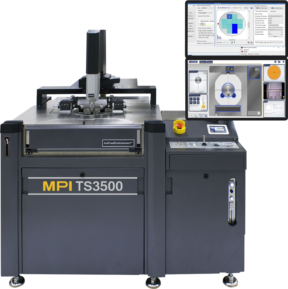
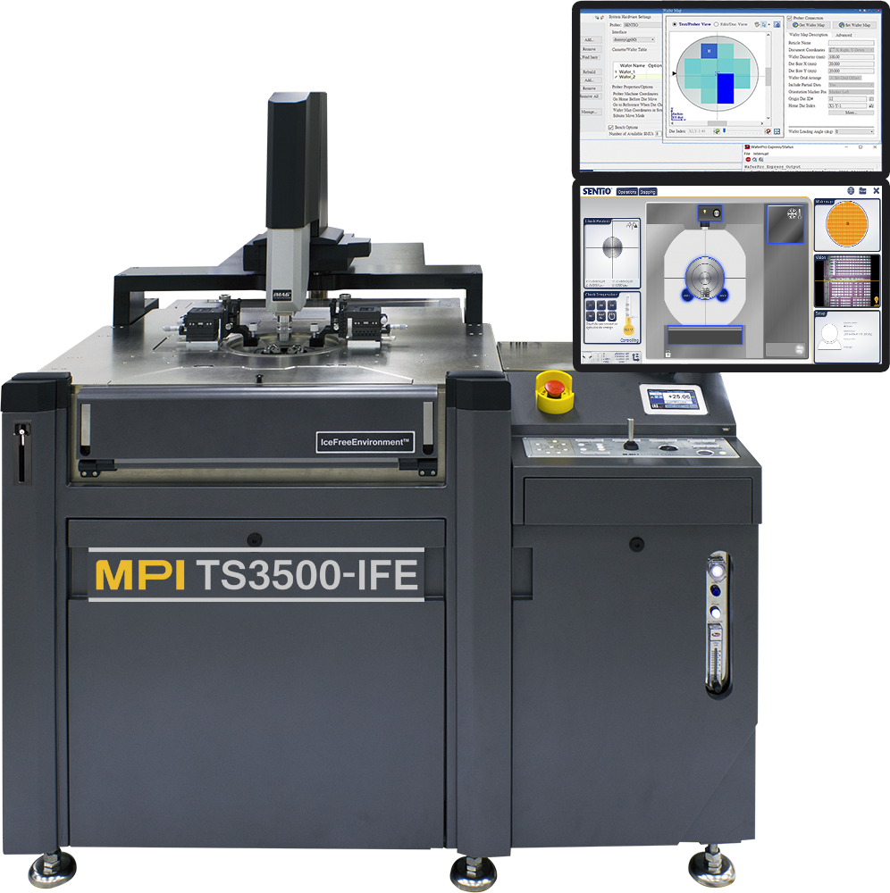
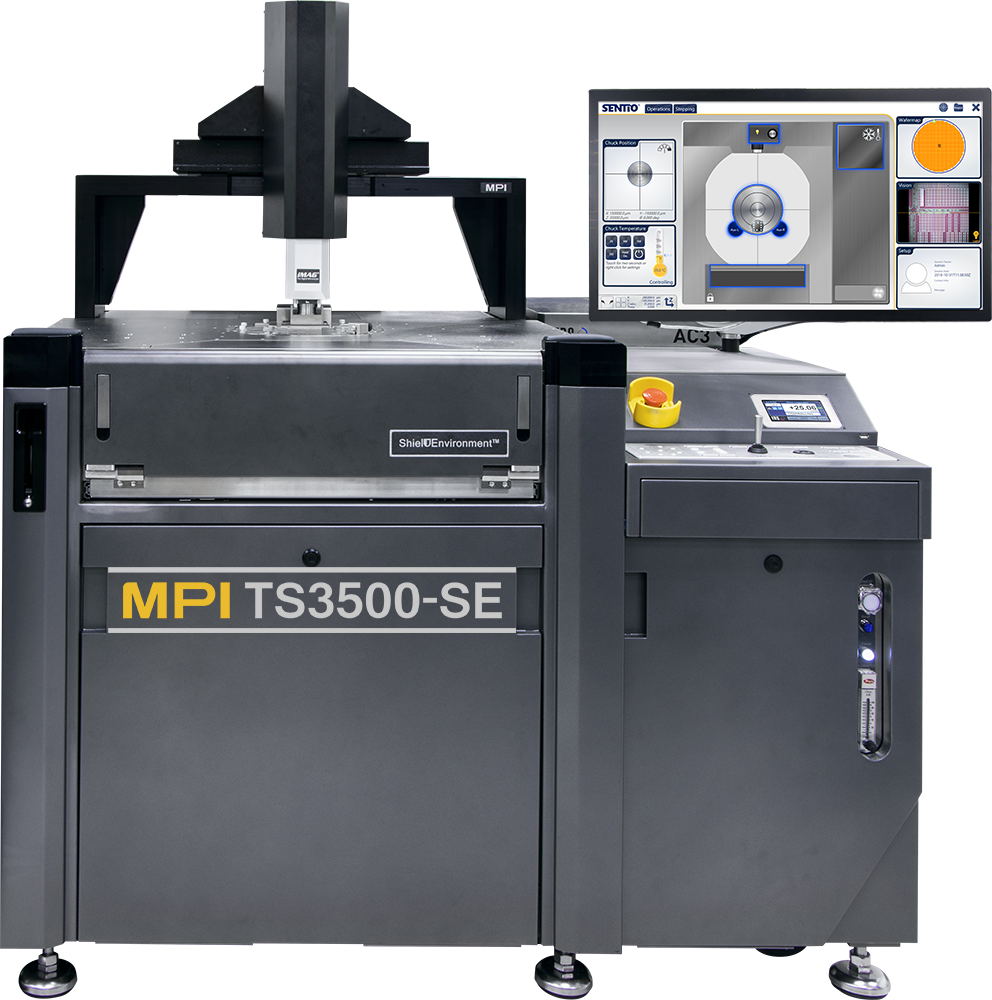
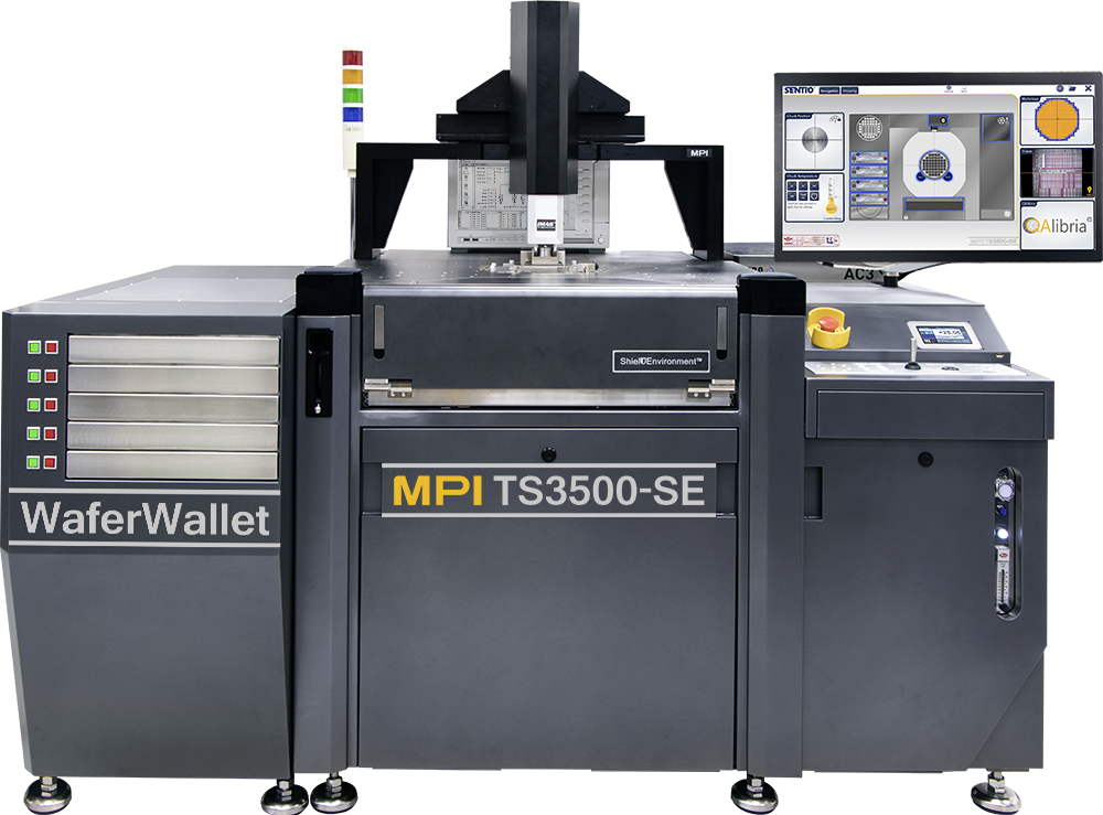
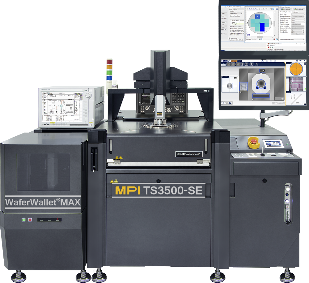
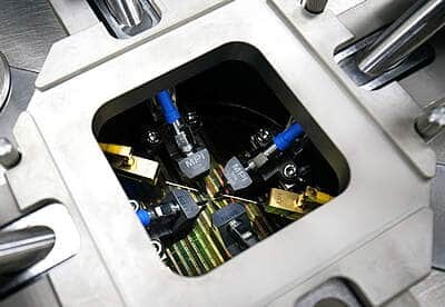
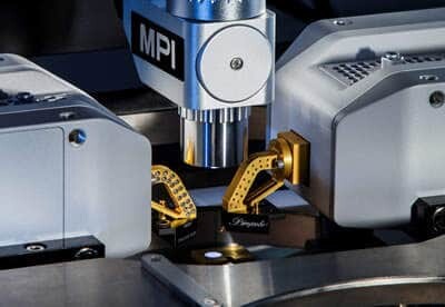
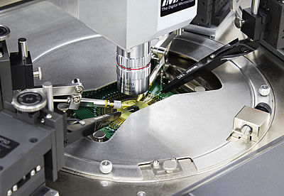
The MPI TS3500 is the entry level probe station enabling automation at lowest cost by using ambient or hot only thermal chucks. In parallel, there is no limitation on the possible options or field upgrades even up to fully shielded, advanced probe station.
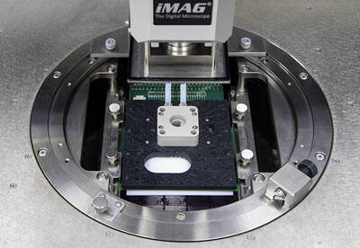
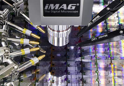
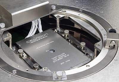
TS3500-IFE and TS3500-SE are equivalent in features to MPI’s well-known and established TS3000-IFE and TS3000-SE 300 mm probe stations with the added fully-automated capability by configuring or upgrading in the field with MPI’s unique WaferWallet® or WaferWallet®MAX or WaferWallet®ULTRA. MPI’s solution is lowering the customer’s overall cost-of-test by providing full automation for less than other vendor’s semi-automated products.
It incorporates MPI advanced technologies, such as PHC™ , as a standard feature, and mDrive™ and/or VCE™ optional or as an upgrade in the field.


