Advanced Semiconductor Test
Understanding Requirements
Relentless Innovation
Reducing Cost of Test
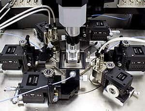
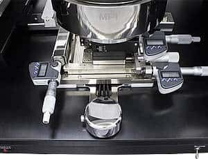
Engineering Probe Systems
Visionary Ideas
Unmatched Value
Quality without Compromise
RF Probes: 26 – 250 GHz
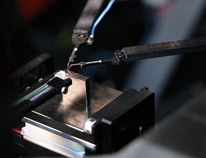
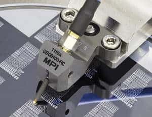
Unique MEMS Based Tips
Reduced Contact Probe
Multi-Contact Probes
High Power