200 mm Automatic Probe Stations

Semi-Automatic Probe Stations | Wafer Test

Semi Automatic probe station | vacuum probe station  | Semi Automatic probe station

200mm Probe Station | Semi Automatic probe station  | Analytic Probers | Manual Probe Station

Probe System | 200mm Probe Stations | Wafer Probe Test | Semi Automatic Probe station 

Wafer Probe Test | Wafer Test  | 200mm Probe Stations | Semi Automatic Probe Station

200mm Probe Station | Wafer Test | Wafer Test | High Power Probe Systems

Probe Stations

200mm Probe Station

Automatic Probe Station

200 mm Automated Probe Station

200mm Wafer Prober

Silicon Photonics

Wafer Probing

200mm Automated Probe Systems

200mm Probe Station

Wafer Probing System

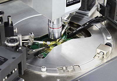
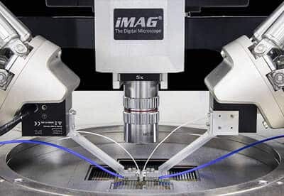
TS2000-IFE Series – MPI Most Versatile 200 mm Platform

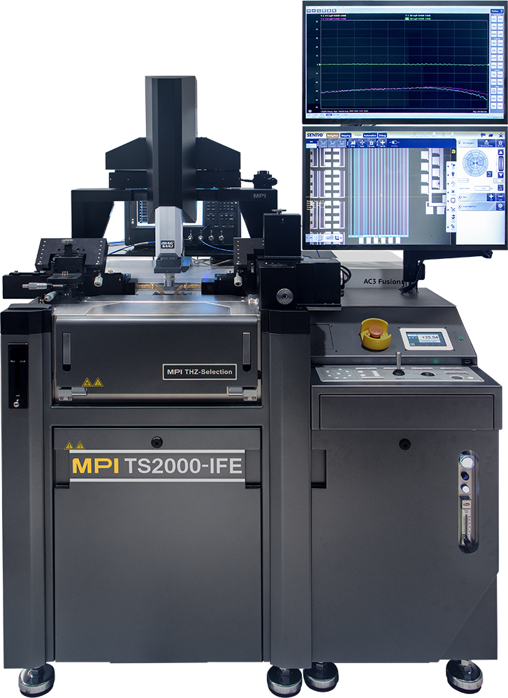
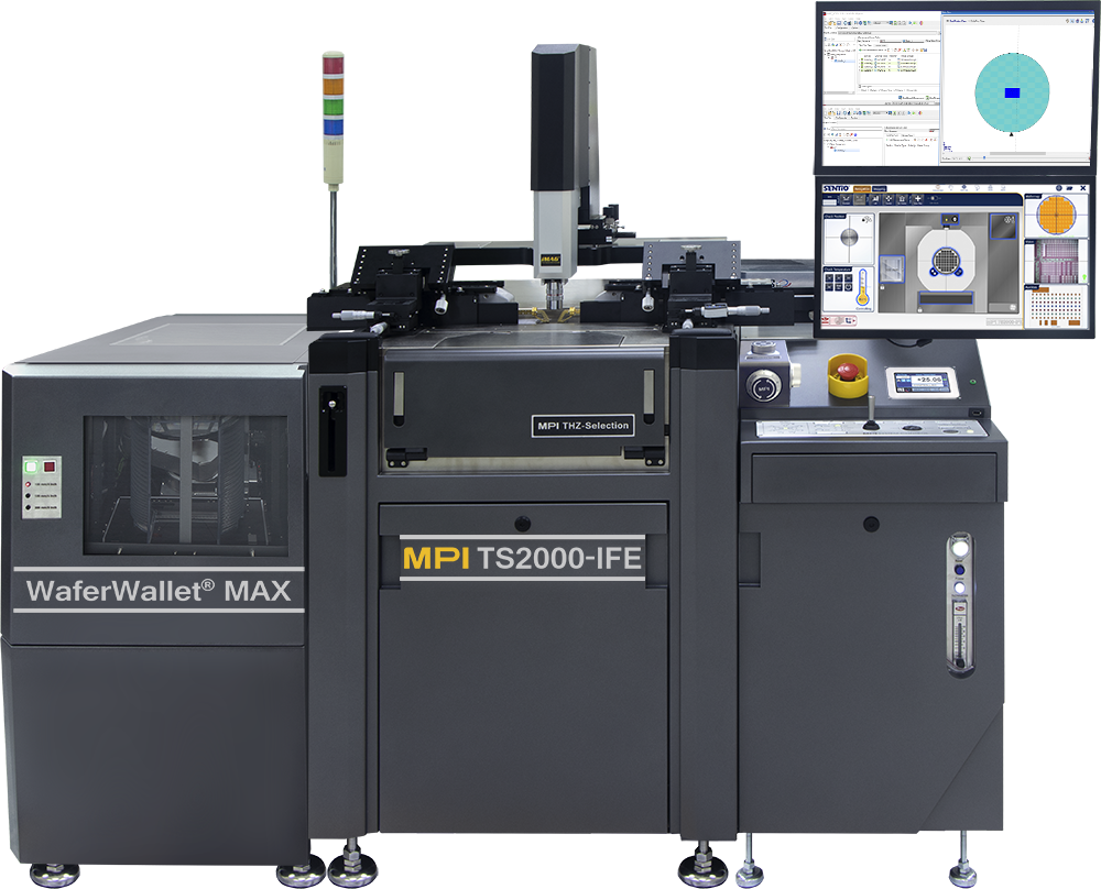
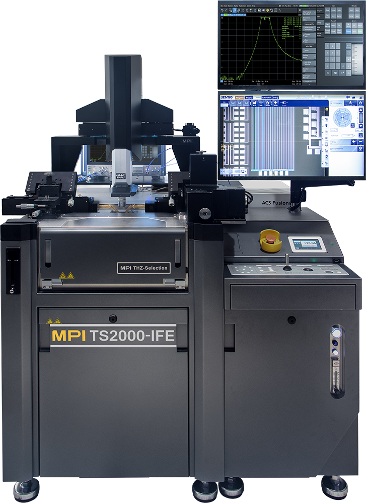
The MPI TS2000-IFE is automated platform which can be converted since the beginning or at any time later in the field to a fully-automatic probe station.

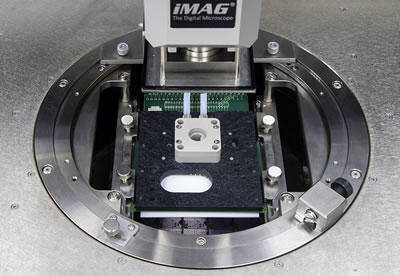
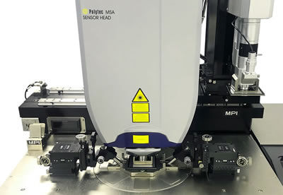
It incorporates MPI advanced technologies, such as PHC™ as a standard feature and mDrive™ or VCE™ optional or as an upgrade.

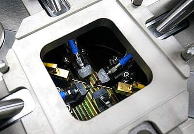
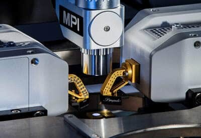
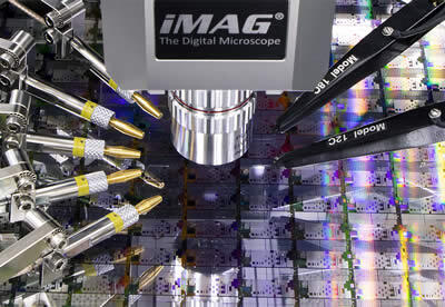
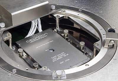
The main applications are  load-pull, RF, mmW,  Silicon Photonics, Design Validation (Product Engineering) or testing of MEMS and other sensors under defined test environment. In combination with WaferWallet® MAX MPI is addressing the transition from Lab to Fab for these specific applications.

Features & Benefits

WaferWallet®MAX – 10x Higher Productivity

MPI’s WaferWallet® MAX is field upgradable and addresses the demand for faster time to market, collecting data from multiple 100 or 150 or 200 mm wafers, and ramping-up tests into a pre-production environment.

With the fastest thermal transition time, reduced soaking time, advanced alignment technologies, cassette or wafer hot-/cold swapping WaferWallet® MAX is increasing system productivity and test cell efficiency up to 10x times.

MPI WaferWallet® MAX

Advanced Alignment

Advanced alignment features such as downward looking off-axis and chuck mounted upward ­ looking cameras make the TS2000-IFE an ideal platform for testing within complex RF, mmW and SiPh measurement configurations. Decades of experience from the MPI Photonics Automation Division making such features highly reliable.

Wafer-ID reader is also available as an option.

IceFreeEnvironment™

Incorporating MPI’s IceFreeEnvironment™ the TS2000-IFE accommodates testing with MicroPositioners and probe cards simultaneously over a wide temperature range of -60°C to +300°C.

The design shortens the signal path thus making the probe station an ideal choice for mmW and/or load-pull applications.

Thermal Chuck Integration

Due to the smart chiller integration, the TS2000-IFE provides optimized footprint for saving valuable space in the lab plus fastest thermal transition time.

MPI and ERS designed together the new PRIME 200 mm chucks family, offering unsurpassed thermal flexibility with reduced soaking time by 60% and the largest variety of thermal ranges and field upgrades.

The thermal system can be operated by using the fully integrated touchscreen display, placed at convenient location in front of the operator for fast operation and immediate feedback.

Integrated Hardware Control Panel

The intelligent hardware control panel is completed integrated into the probe system and is designed based on decades of experience and customer interactions to provide faster, safer and convenient system control and test operation. The keyboard and mouse are strategically located to control the software if necessary and will also control the Windows® based instrumentation.

ERS Patented AC3 Cooling Technology Incorporated

These chucks incorporate the patented AC3 cooling technology and self-management system to purge the MPI ShielDEnvironment™ using recycled cooling air, thus drastically reducing air consumption 30% to 50% compared to other systems on the market.

ERS Patented AC3 Cooling Technology

MPI SENTIO®

By using a novel approach based on simplicity and truly intuitive operation, MPI was first to develop a revolutionary multi-touch prober control software suite to address today’s challenges of operating complex probe test systems.

MPI goal is to save significantly training time and makes the operators’ life as easy as possible, even by operating the fully-automatic TS2000-IFE probe stations.

MPI Prober Control Software Suite SENTIO®

Field Application Engineer

Job Location: San Jose, CA

Job Duties:

  • Assist in developing HW and SW measurement methodologies/solutions for analytical wafer probe solutions with signal applications from DC to millimeter wave frequencies as well as Silicon Photonics (SiPH);
  • Collaborate with customers on their measurement challenges, and provide applications specific product training;
  • Provide pre- and post-sale support to AST, customers, service department, and the sales channel developing HW and SW measurement solutions for analytical wafer probe stations;
  • Define application-specific solutions based on customer-provided device data and facilitate both customer and divisional teams to successful results;
  • Perform product training seminars for customer and sales channels as well as participate in trade shows and technical seminars;
  • Make recommendations regarding product improvement, new products, and quality enhancement;
  • Author, document, publish, and present measurement solutions via Seminars, Applications Notes, Briefs, and White Papers;
  • Prepare, plan, and assist with customer product demonstrations that highlight value-based differentiation of AST product offerings;
  • Develop unique and individual customer presentations designed to professionally position the MPI brand in the North American market and deliver formal presentations to customers.

Job Requirements:

Master’s degree in Electrical Eng., Electronics Eng., Physics, or Photonics; Must possess 6 months of relevant work experience; Travel to customers’ sites in US and headquarters in Taiwan is required.

Send resume to: MPI America, Inc., 2360 Qume Drive, Suite C, San Jose, CA 95131, Attn: Janet Chiang