
MPI Automated Probe Systems
Main Applications
MPI’s 200 mm and 300 mm automated probe systems are dedicated and designed to address current and future requirements for all facets of Device Characterization for Modeling and Technology/Process Development, Failure Analysis, Design Verification, IC engineering, Wafer Level Reliability as well as special requirements for MEMS, High Power, RF and mmW device testing.
24/7 Reliability
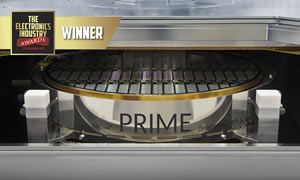
The Advanced Semiconductor Test engineering probe systems incorporate the same hardware controller as the well-established, market leading Photonics Automation probe systems that has global installed base of more than 10,000 systems. Time tested and proven in demanding 24/7 operations, MPI is now introducing such capabilities and systems reliability into the Engineering Market.
Products
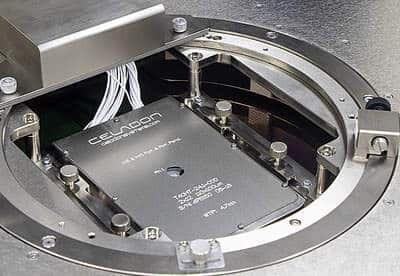
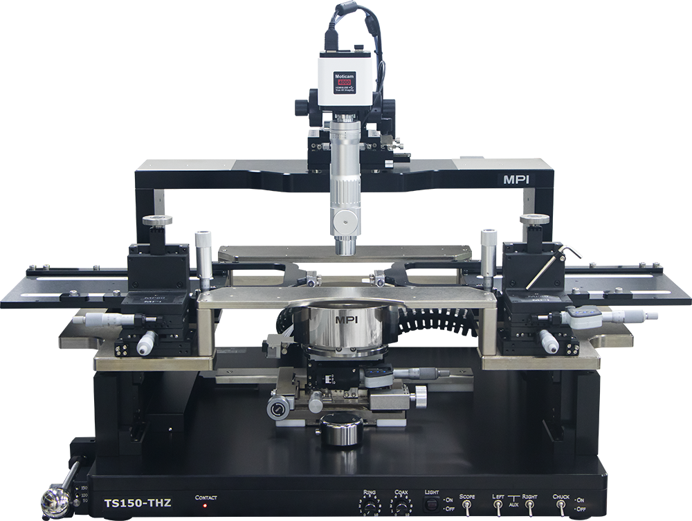
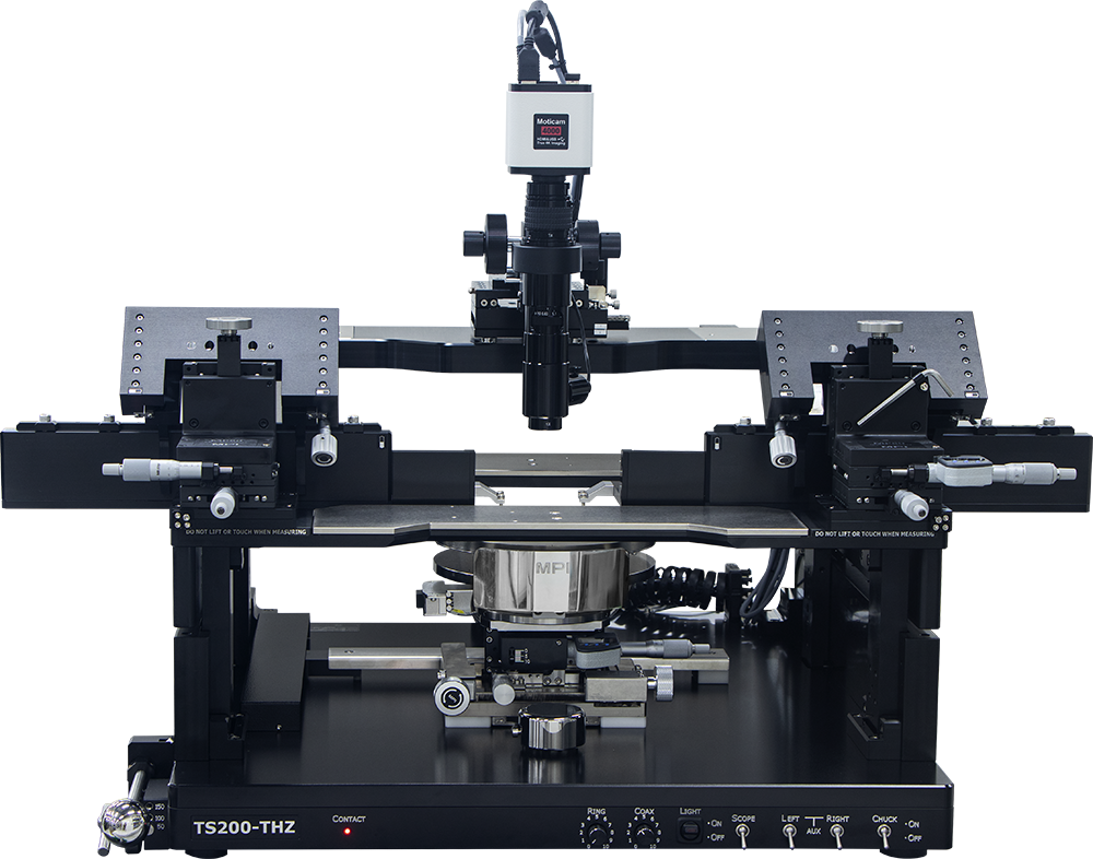
The TS2000 and TS3000 are the probe systems which can be configured with ambient to hot chucks up to 300°C.
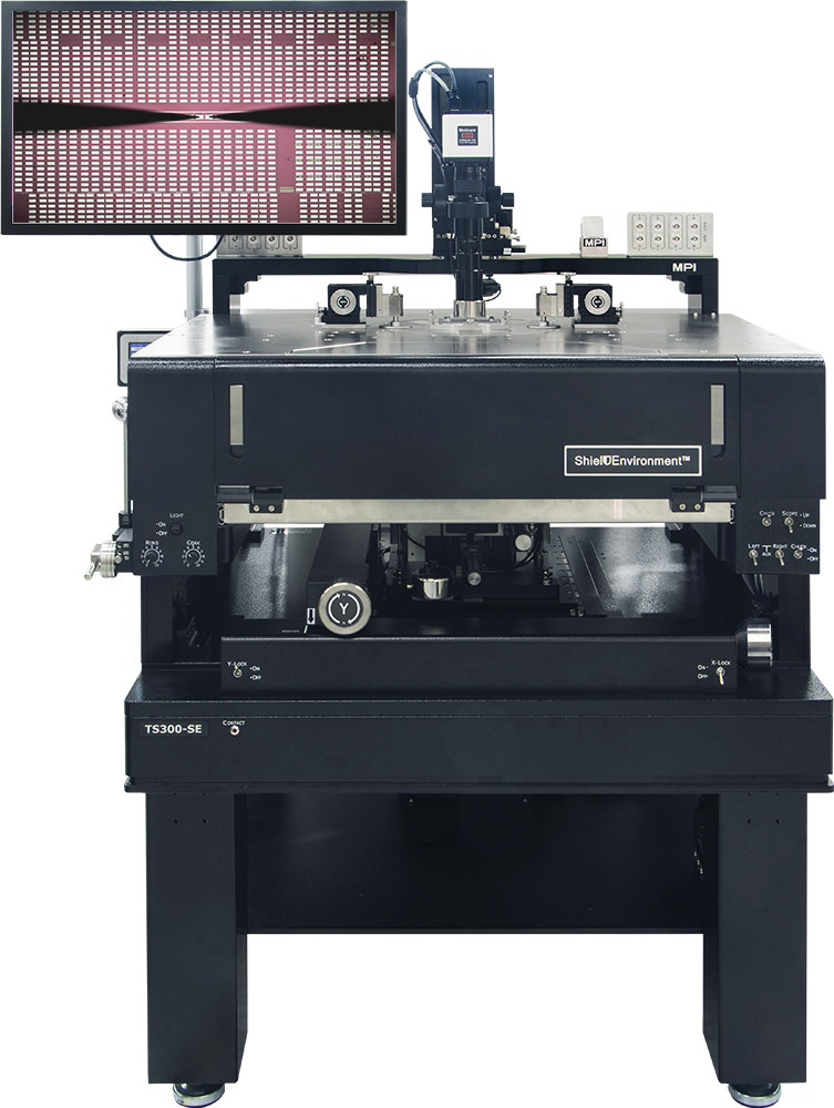
The TS2000-SE and TS3000-SE can be configured at extended temperature ranges from -60°C to +300°C and where TS2000-SE is the advanced probe system equipped with automated single wafer loader for convenient wafer swap at any temperature.
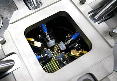
The SE stands for MPI ShielDEnvironment™ – a local environment chamber providing an excellent EMI- and light-tight shielding for ultra-low noise measurements.

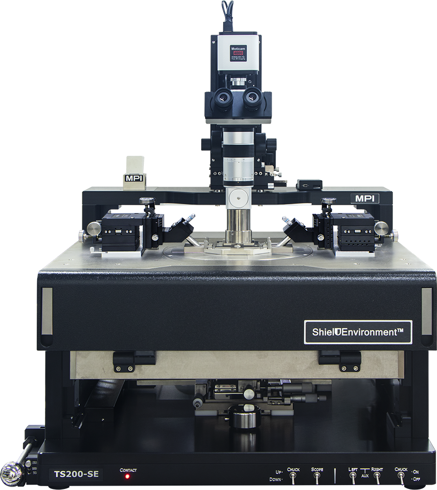


TS2000-SE
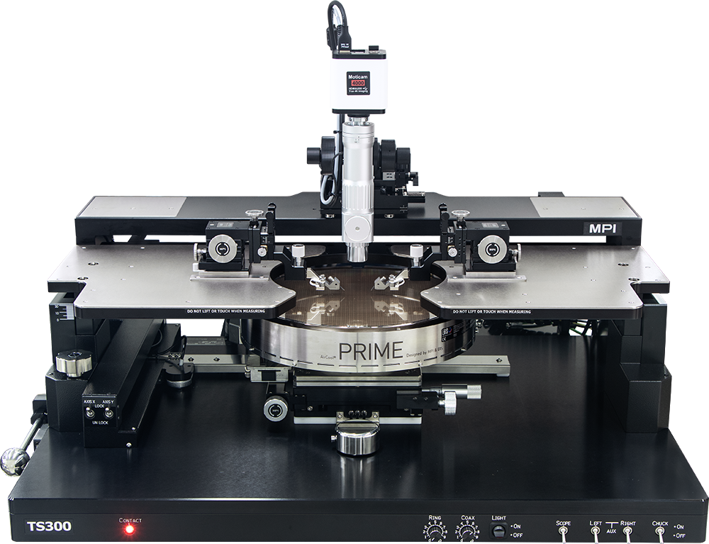
TS3000
TS3000-SE
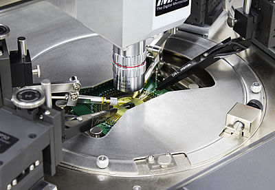
SiPH Probe System
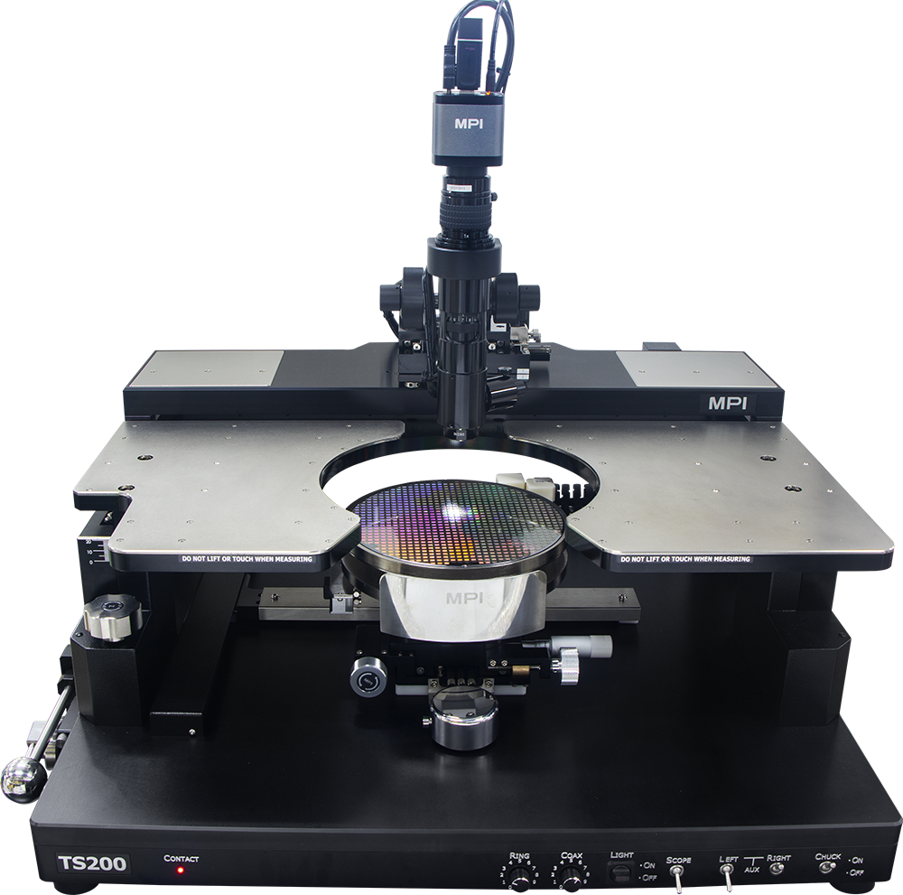
TS2000
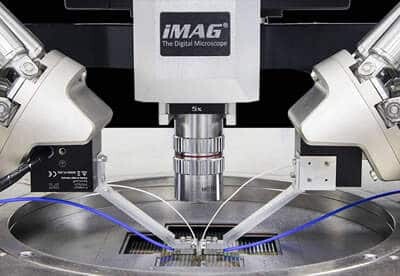
TS2000-IFE


TS150-HP & TS200-HP
TS2000-DP Probe System
TS2000-HP Probe System
TS3000-HP
TS3500-HP
TS2500-DP


TS3500-SE with WaferWallet®
TS2000-IFE with WaferWallet®MAX
TS2500 Series
TS2500-SE


Chuck Systems
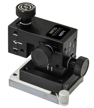
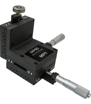
MicroPositioners
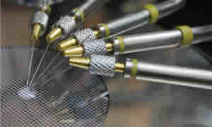
DC & RF Probe Arms
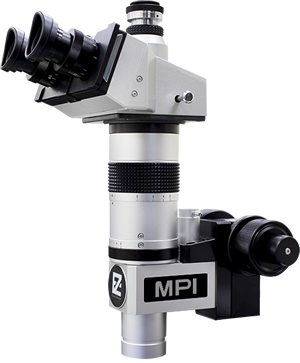
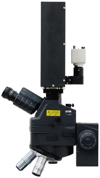
Optics
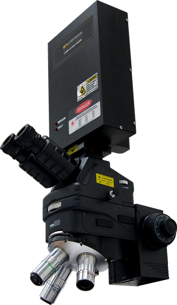
Laser Cutter
TITAN™ RF Probes
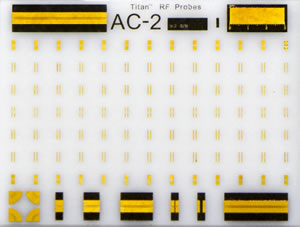
Calibration Substrates
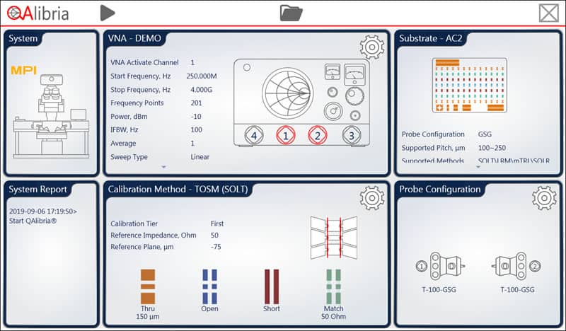
RF Calibration Software
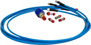
RF Accessories
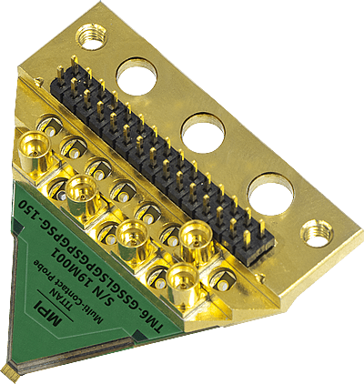
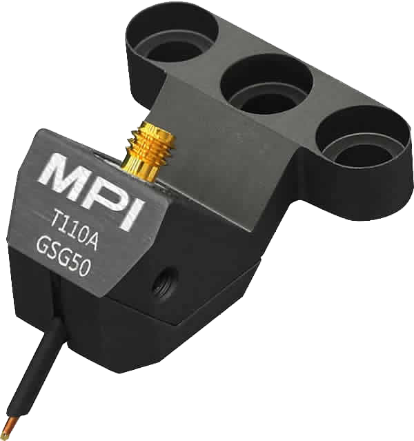
TITAN™ Multi-Contact Probes