Semi Automatic Probe Stations | 200mm Probe Stations  | Semi Automatic probe | 200 mm Wafer Prober | Semi Automatic probe | 200mm Probe Station | Probe Systems

200mm Probe Station | Probe Systems

microwave probe | Probe Station

Semi-Automatic Probe Stations | 200 mm Wafer Prober

Automated Test over Multiple Temperatures ATMT™

True to our mission of making complex probe station operation as intuitive as possible, minimizing training costs, and continuously focusing on reducing cost of test, MPI designed unique and cost-effective technologies, that enable Automated Test over Multiple Temperatures ATMT™. In combination with MPI’s WaferWallet® or WaferWallet®MAX, Device Modeling and Wafer Level Reliability engineers will benefit from these features to generate significant more measurement data. It shortens the time-to-market for new product developments, offering a competitive advantage for our customers, where they can react faster to market changes and always be one step ahead of their competitors.

Features & Benefits

ATMT™ DC

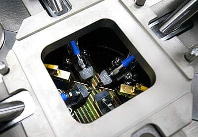
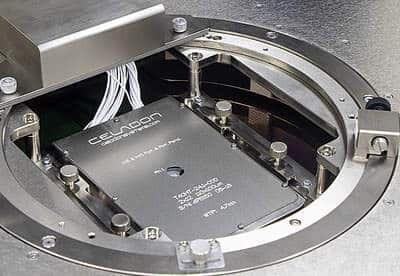
For DC over temperature measurements, Device Modeling and Wafer Level Reliability engineers are commonly using Celadon’s, high temperature, low leakage probe cards. MPI and Celadon are finally offering leading edge, complete measurement solutions, enabling Automated Test over Multiple Temperatures ATMT™ DC at wide temperature range: -60…300°C.

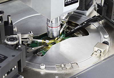
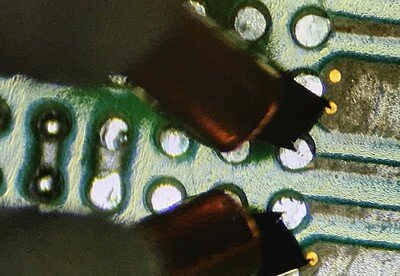
For the case of a few measurements performed with MicroPositioners, MPI has developed thermally stable Kelvin probes that allow Automated Test over Multiple Temperatures ATMT™ at -40 to 175°C.

ATMT™ RF

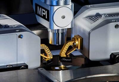
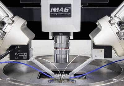
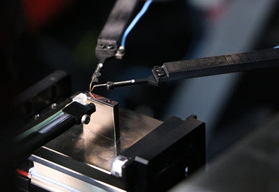
MPI’s SmartCarrier™ uniquely combines different materials that automatically compensate for the lateral expansions of the RF probes without the need for complex software or programmable MicroPositioners*.

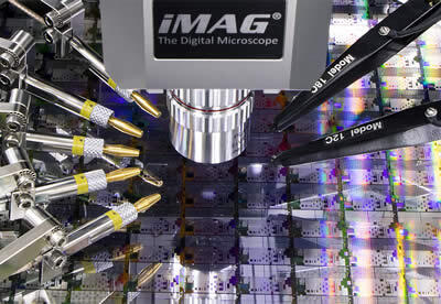
SENTIO®‘s new patent-pending ContactSense™ image processing can determine the new contact positions on-the-fly with an accuracy of a few micrometers, completing MPI’s Automated Test over Multiple Temperatures ATMT™ RF.

* One programmable MicroPositioner is recommended for automated RF calibration by using QAlibria®

Field Application Engineer

Job Location: San Jose, CA

Job Duties:

  • Assist in developing HW and SW measurement methodologies/solutions for analytical wafer probe solutions with signal applications from DC to millimeter wave frequencies as well as Silicon Photonics (SiPH);
  • Collaborate with customers on their measurement challenges, and provide applications specific product training;
  • Provide pre- and post-sale support to AST, customers, service department, and the sales channel developing HW and SW measurement solutions for analytical wafer probe stations;
  • Define application-specific solutions based on customer-provided device data and facilitate both customer and divisional teams to successful results;
  • Perform product training seminars for customer and sales channels as well as participate in trade shows and technical seminars;
  • Make recommendations regarding product improvement, new products, and quality enhancement;
  • Author, document, publish, and present measurement solutions via Seminars, Applications Notes, Briefs, and White Papers;
  • Prepare, plan, and assist with customer product demonstrations that highlight value-based differentiation of AST product offerings;
  • Develop unique and individual customer presentations designed to professionally position the MPI brand in the North American market and deliver formal presentations to customers.

Job Requirements:

Master’s degree in Electrical Eng., Electronics Eng., Physics, or Photonics; Must possess 6 months of relevant work experience; Travel to customers’ sites in US and headquarters in Taiwan is required.

Send resume to: MPI America, Inc., 2360 Qume Drive, Suite C, San Jose, CA 95131, Attn: Janet Chiang