
MPI NoiseShield™

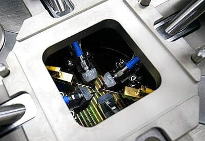
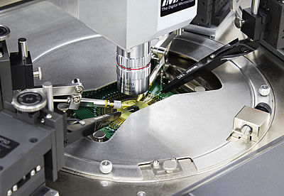
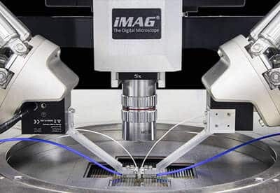
MPI probe stations equipped with ShielDEnvironment™ – high performance local environmental chamber – such as TS200-SE, TS300-SE, TS2000-SE, TS3000-SE or TS3500-SE provide excellent EMI and light-tight shielded test environment for ultra-low noise measurements.
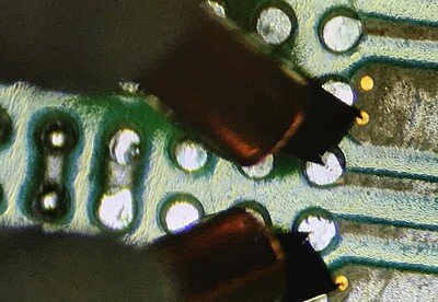
Best in class specification of MPI ShielDEnvironment™ are defined under real life testing conditions, which include four Kelvin DC probes. It makes MPI Shielded probe systems the benchmark for 1/f (Flicker) Noise and RTN measurements.
Features & Benefits
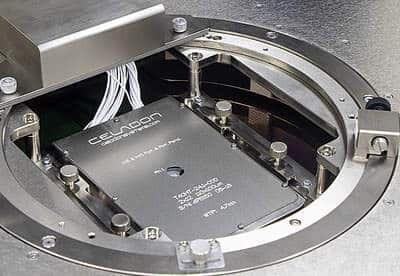
Extensive Shielding
The NoiseShield™ option provides shorter cable lengths to reduce parasitic capacitance to maximize the test system roll-off frequency. It also reduces external magnetic field influences on the measurement results and makes the 1/f, RTN setup more robust and test lab location less-independent.
The NoiseShield™ DUO enables dual channel, parallel measurements of 1/f noise and RTN with two pre-amplifier units of Primarius 9812DX and therefore twice increase the measurement volume at the same given time.


Seamless Integration
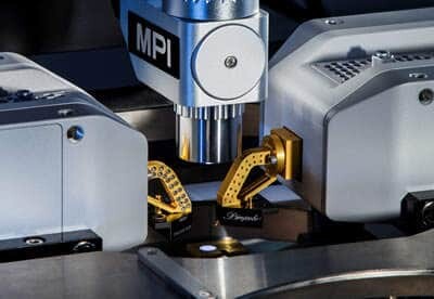
Low impedance cables, low-impedance system’s grounding and ferrite cores on the unique MPI Kelvin probes are part of the delivery in order to make the probe station completely “invisible” and to achieve measurement results to reach the limit of the instrumentation noise floor.
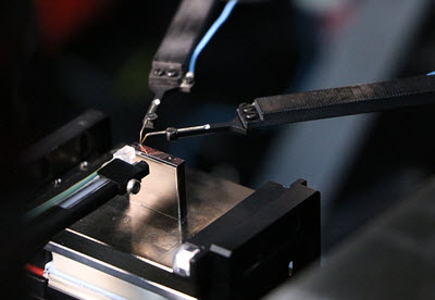
The NoiseShield™ design provides convenient set-up as well as, integrating ProPlus 9812DX High Precision LNA very close to DUT and supports DC or RF pad design.
For more please see here.
