
MPI TS200-SE Probe System


The MPI TS200-ShielDEnvironment™ (TS200-SE) is designed to ensure advanced EMI/RFI/light-tight shielding, ultra-low noise, low leakage measurement capabilities in a temperature range from -60 to +300°C.
Features & Benefits
ShielDEnvironment™
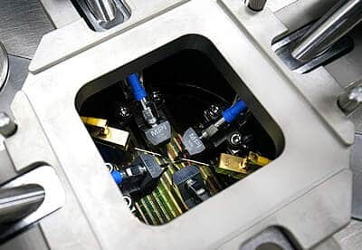
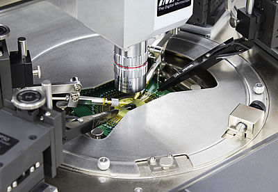
MPI ShielDEnvironment™ is a high performance local environmental chamber providing excellent EMI- and light-tight shielded test environment for ultra-low noise, low capacitance measurements.

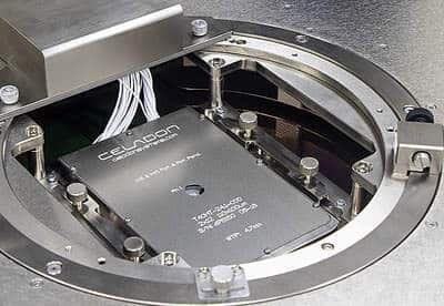
ShielDCap™
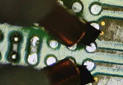
A fully configurable part of the MPI ShielDEnvironment™ which allows up to 4-port RF or up to 8-ports DC/Kelvin or a combination of those configurations.
Easy to reconfigure with convenient shielding that is MPI ShielDCap™ – a lot of little things which make the difference in simplifying day by day operations.
The complete ShielDCap™ is easily replaceable with the EMI-Shielded version of a probe card holder.

IceFreeEnvironment™
Incorporating MPI’s IceFreeEnvironment™ the TS200-IFE accommodates testing with MicroPositioners and probe card simultaneously over a wide temperature range of -60°C to +300°C.
The design shortens the signal path thus making the probe station an ideal choice for mmW and/or load-pull applications.


THZ Selection
The MPI TS200-IFE THZ-Selection is based on MPI’s most versatile 200 mm platform TS200-IFE and converts it into a dedicated, RF, mmW , THZ and load-pull probe station, as first to market without compromising measurement directivity and accuracy at wide temperature ranges from -60°C to +300°C.

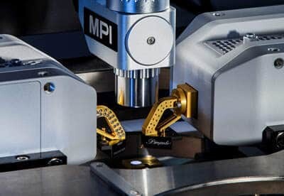
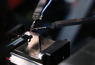
Air-Bearing Stage
The MPI unique air-bearing stage design, with simple single-handed puck control, provides unsurpassed convenience of operation for fast XY navigation and quick wafer loading without compromising accurate and fine positioning capability with the additional fine and accurate 25x25mm XY-Theta micrometer movement.


Unique Platen Lift
with Probe Hover Control™
The repeatable (1 μm) platen lift design has three discrete positions for contact, separation (300 μm), and loading (3 mm). The lift includes a safety lock rotation utility which prevents accidental platform descent. These features offer unparalleled functionality and are standard offerings for the MPI TS200-SE manual probe system. Prevention of unexpected probe or wafer damage is critical to system design and provides intuitive control, accurate contact positioning, safe set-ups, and easy step and repeat functionality.
Unique Chuck Z Adjustment
TS200-SE incorporates in addition to the air bearing XY stage – 5 mm Z chuck adjustment in µm resolution for fine and accurate contact / over-travel control or probe card drop tip correction.
A 1 mm scale indicator provides easy feedback to the operator. 20 mm pneumatic lift in addition offers easy and continent loading / unloading procedure.


Various Chuck Options
The TS200-SE is available with various chuck options to meet different budgets and application requirements:
-
- Ambient Chucks: Coaxial, Triaxial or RF with two auxiliary chucks built in ceramic material for accurate RF calibration
- Various ERS AirCool Chucks from -60°C to 300°C

Thermal Control Integration
The wafer loading door is simply locked at any temperatures below 15°C – this unique feature makes TS200-SE the safest manual probe station in the market.
Furthermore, the thermal chuck can be operated by using the fully integrated touchscreen display, placed at convenient location in front of the operator for fast and operation and immediate feedback.

ERS Patented AC3 Cooling Technology Incorporated
These chucks incorporate the ERS patented AC3 cooling technology and its air management system to purge the MPI ShielDEnvironment™ directly from “already used” air – reducing dry air consumption up to 30 to 50% as compared to other systems on the market.

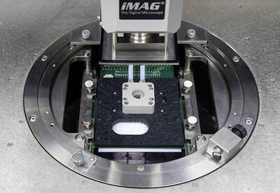
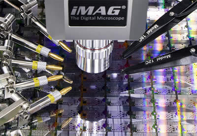
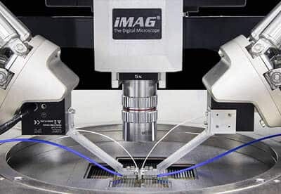
Various Optic Options
MPI Optics are available with a choice between a single tube MPI SuperZoom™ SZ10, the MegaZoom™ MZ12 with up to 12x optical zoom and more than 42 mm working distance or EeyZoom™ EZ10 – the 10x optical zoom optic with ergonomic 20x eyepieces, 90 mm working distance and down to 2 µm optical resolving power.


Unique Upgrade Path
The modular design of theTS200-SE modular creates a unique upgrade path. All TS200-SE probing accessories, such as thermal chucks, microscope and positioners, can be upgraded or reconfigured to variety of application requirements covering tool lifespan for increasingly low cost of ownership.
The MPI TS200-SE probe systems with ShielDEnvironment™ provides maximum EMI shielding and allows for low noise device on-wafer measurements for wide verity of applications such as Device Characterization and Modeling , RF/Microwave , Wafer Level Reliability , Failure Analysis , Design Validation , and High Power .