MPI Engineering Probe Systems

Variety of Test Systems

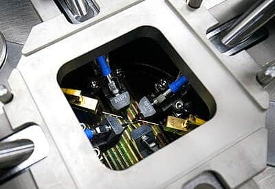
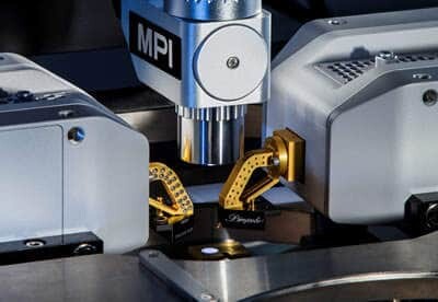
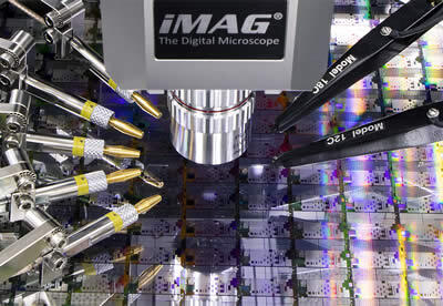
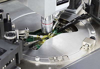
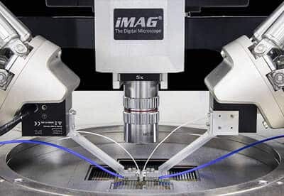
The MPI Advanced Semiconductor Test Division is providing a wide range of engineering probe systems addressing the specific requirements of various market segments and applications such as Device Characterization for modelingFailure AnalysisDesign Verification, IC engineeringWafer Level Reliability as well special requirements for MEMS, High PowerRF and mmW device testing.

Wafer Probing

Our Mission

The AST mission is to provide engineering Test Solutions with a Modest Price Structure that does not compromise quality in any way.

We guarantee the highest value for the price on all comparable products within our market – period.

The TS series modular design concept allows a unique upgrade path towards reduced cost of ownership.
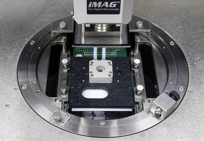
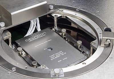
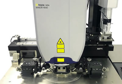
blank

Relentless Innovation

MPI Advanced Semiconductor Test Division’s ability to understand customer and market requirements FAST and having the talent to turn those learnings into INNOVATIVE, never seen before Engineering Probe Systems, are the key differentiators to other products on the market.

As technology and innovation leaders MPI Engineering Probe Systems are pioneering in many areas with features only found on Advanced Semiconductor Test Division products.

Integration

The thoughtful and all-inclusive approach of integrating measurement instruments, high-power probes, Kelvin Probes, RF Probes, RF Calibration Software and Thermal Chucks, and variety of different Accessories clearly demonstrates the exceptional value of MPI engineering probe systems.

MPI ShielDCap™

Field Application Engineer

Job Location: San Jose, CA

Job Duties:

  • Assist in developing HW and SW measurement methodologies/solutions for analytical wafer probe solutions with signal applications from DC to millimeter wave frequencies as well as Silicon Photonics (SiPH);
  • Collaborate with customers on their measurement challenges, and provide applications specific product training;
  • Provide pre- and post-sale support to AST, customers, service department, and the sales channel developing HW and SW measurement solutions for analytical wafer probe stations;
  • Define application-specific solutions based on customer-provided device data and facilitate both customer and divisional teams to successful results;
  • Perform product training seminars for customer and sales channels as well as participate in trade shows and technical seminars;
  • Make recommendations regarding product improvement, new products, and quality enhancement;
  • Author, document, publish, and present measurement solutions via Seminars, Applications Notes, Briefs, and White Papers;
  • Prepare, plan, and assist with customer product demonstrations that highlight value-based differentiation of AST product offerings;
  • Develop unique and individual customer presentations designed to professionally position the MPI brand in the North American market and deliver formal presentations to customers.

Job Requirements:

Master’s degree in Electrical Eng., Electronics Eng., Physics, or Photonics; Must possess 6 months of relevant work experience; Travel to customers’ sites in US and headquarters in Taiwan is required.

Send resume to: MPI America, Inc., 2360 Qume Drive, Suite C, San Jose, CA 95131, Attn: Janet Chiang