
Design Validation and IC Engineering
")
MPI Definition
IC design validation is critical to the success of today’s semiconductor manufacturing process.
Large amount of test data has to be generated during post-silicon system validation. Complex ICs show their problems only after certain days or weeks of testing.
In addition to electronic design automation (EDA) design verification tools, built-in-self-test (BIST) and design-for-test (DFT) methods, IC manufacturers are using a variety of methods to validate first silicon examples. This includes testing with engineering probe systems by using variety of instrumentation, automated test equipment (ATE) and dedicated engineering validation systems.
Major Requirements
When doing measurements for IC engineering and design validation, engineers are challenged by the need for system configuration changes of test instrumentation such as DC and RF power sources and meters, oscilloscopes, and/or VNAs. Compounding the issue is measurement over temperature, high-impedance, frequency ranges and driving the IC with high pin-count probe card. Cable interface to ATE is very common too.
The testing and defects identifications techniques during Design Validation are very similar with the Failure Analysis, therefore:
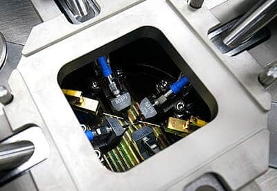
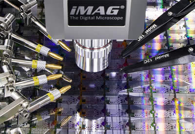
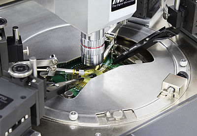
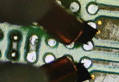
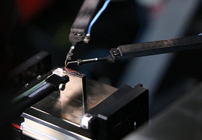
- The IC is fired-up by probe card and the micro-probing has to be done via several single probes simultaneously
- Such probe card are usually customized and very often very long (>13”) by containing active components, close to DUT are common too.
- The IC is fired-up by probe card and the micro-probing has to be done via several single probes simultaneously
- Such probe card are usually customized and very often very long (>13”) by containing active components, close to DUT are common too.
MPI Solutions
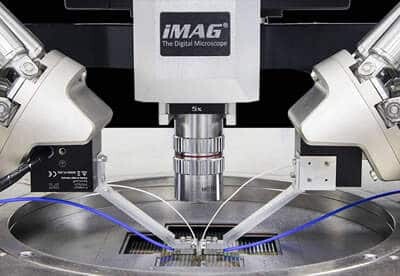
The flexible design of MPI Engineering Probe Systems supports DC, triaxial and RF Chucks from 50 to 300 mm sizes with wide temperature ranges, entry-level and high-end DC and RF MicroPositioners, single-tube microscopes and Optic options with wide working distances, provide the ideal solution for any measurement need and budget capabilities.
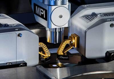
MPI TS3000 probe systems, offer uniquely the simultaneous use of probe card and MicroPositioners (DUT driving & internal signal measurements), especially at temperatures down to negative 60°C.
The low platen to chuck distance makes the Picoprobing very convenient.
DarkBox option offer light-tight design validation of Image sensors as example.
MPI’s complete solutions for RF Probes ICs provide the perfect environment for precision RF measurements and calibrations up to 110 GHz by employing MPI’s calibration software QAlibria® and MPI RF and Microwave probes.
Dual TITAN™ probes with GSGSG and GSSG is the ideal choice for the measurement mmW differential ICs. MPI also offers broadband active probes with replaceable probe tips and high input impedance for precise oscilloscope measurements.