
MPI Manual Probe Systems
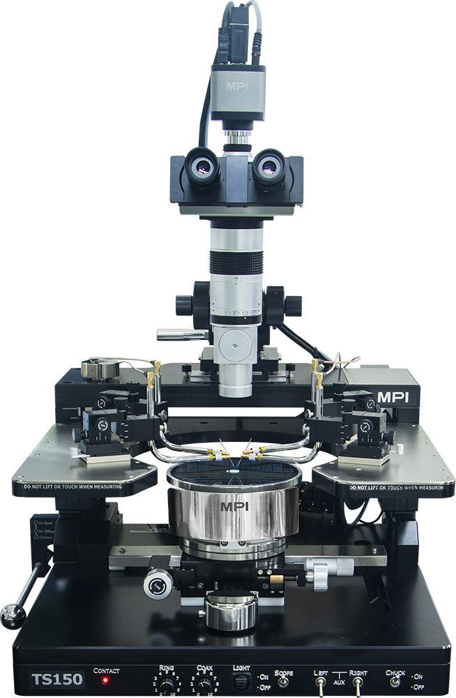
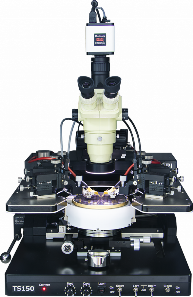
MPI TS150 - 150 mm Manual Probe System
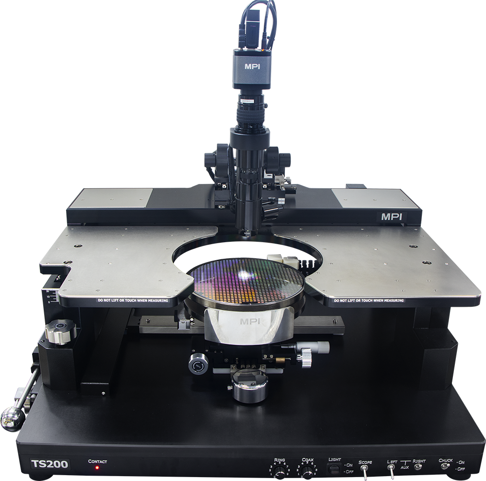
MPI TS200 - 200 mm Manual Probe System
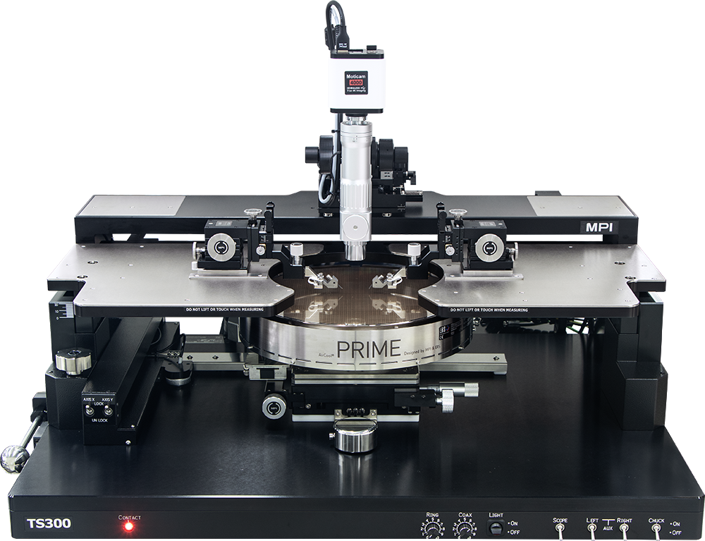
MPI TS300 - 300 mm Manual Probe System
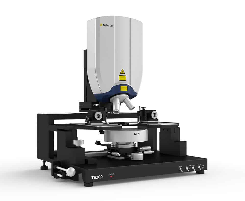
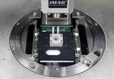
MPI TS200 with Polytec MSA600 Motion System Analyzer
Standard Open Systems
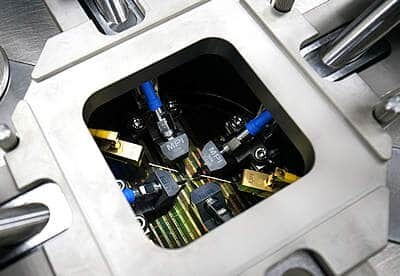
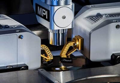
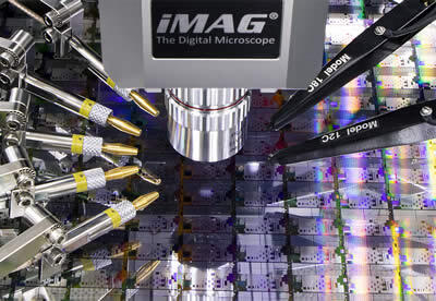
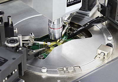
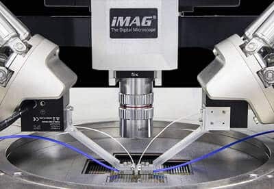
MPI TS150, TS200 & TS300 manual probe systems are open, easy to use and cost effective yet highly accurate. These systems are designed for precision analysis of substrates and wafers up to 150, 200 and 300mm.
They may be configured to support a wide variety of applications such as Failure Analysis , Design Validation/IC Engineering , Wafer Level Reliability , High Power , Device Characterization , MEMS and Signal Integrity as well.
High Power Systems
The MPI TS150-HP and TS200-HP probe systems are specifically designed for on-wafer high power device characterization testing up to 10 kV and 600 A. Dedicated chuck designs, connectors and cables are engineered to achieve low contact resistance measurements of power semiconductor under wide range of temperatures.
TS150-HP
TS200-HP
Dedicated Systems for mmW and THz Application
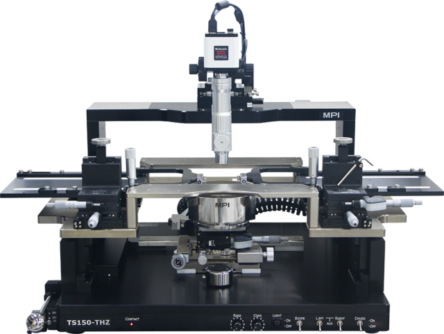
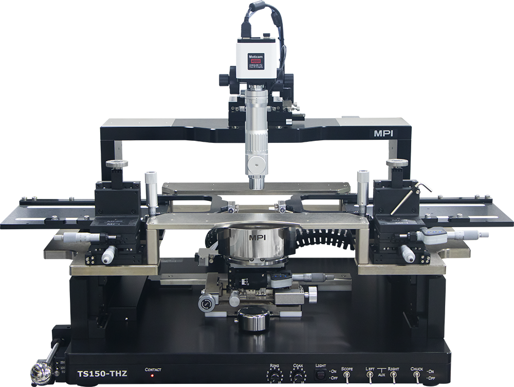
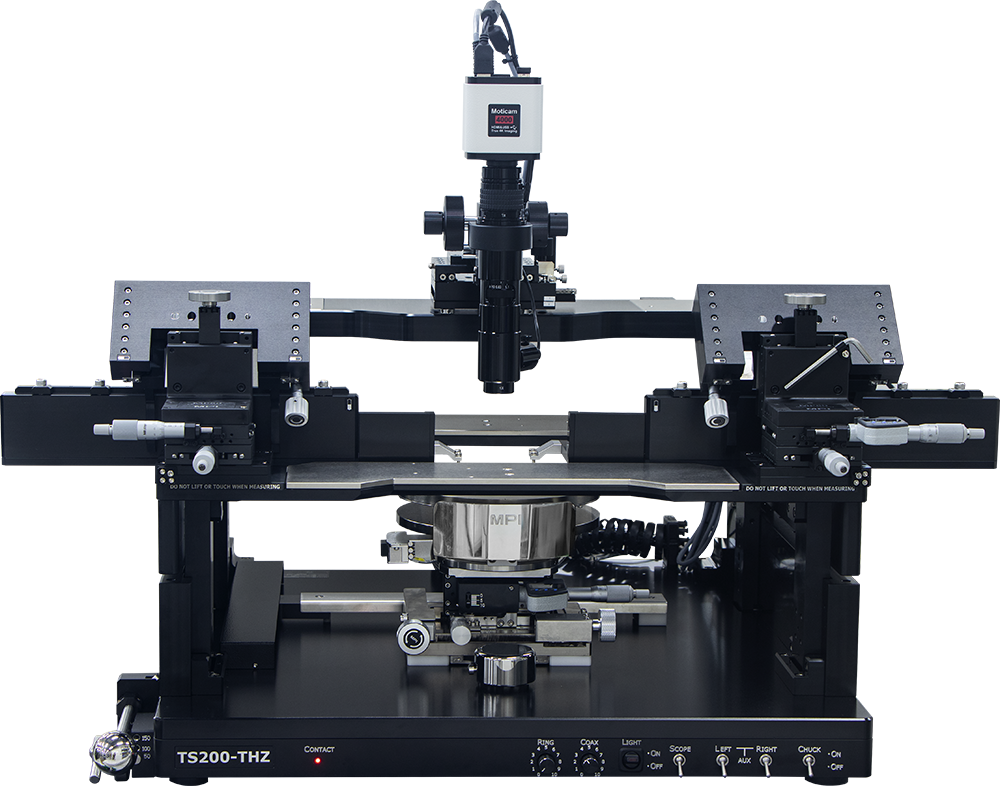
MPI TS150–THZ engineering probe system is a dedicated, cost effective, manual probe system designed especially for precision analysis of substrates and 150 mm wafers in sub THz range. The system is extremely stable, with a large probe platen, and a low-profile design. Each of these essential elements are required to support a wide variety of RF and mmW applications such as broadband up to 220 GHz, banded solutions up to 1.1THz, load-pull and RF noise.
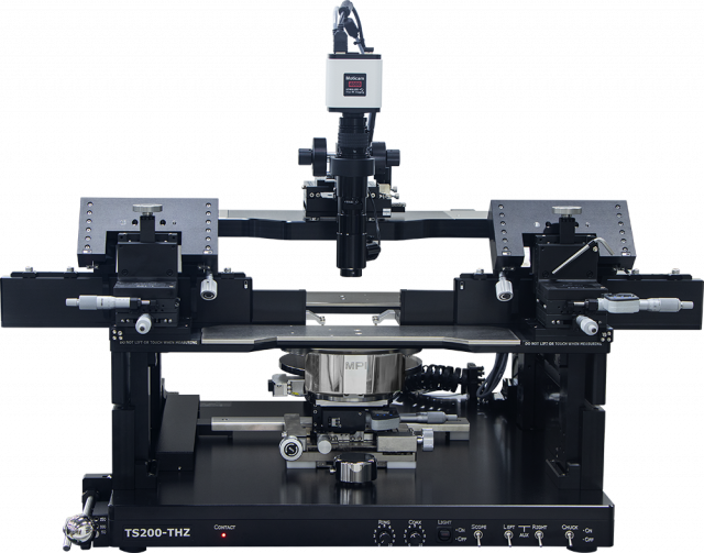
TS150-AIT and TS200-THZ probe system expand MPI one-of-a-kind system solutions for emerging THz applications by adding active impedance tuner integrations on the same probe stations. These two systems are the industry’s first explicitly designed 150 mm and 200 mm probe systems providing accurate tests for the combination of requirements for mm-wave, THz, and automated impedance tuner applications with best possible measurement directivity.
TS150-THZ
TS200-THZ
Shielded Systems
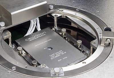
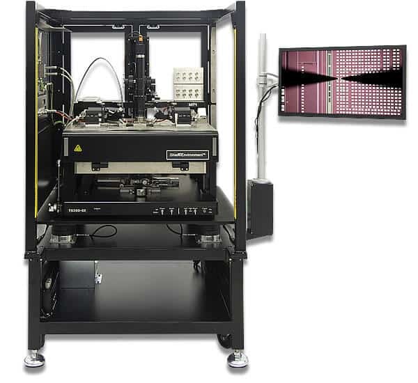
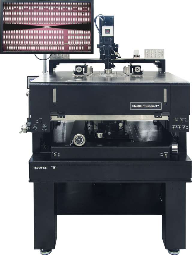
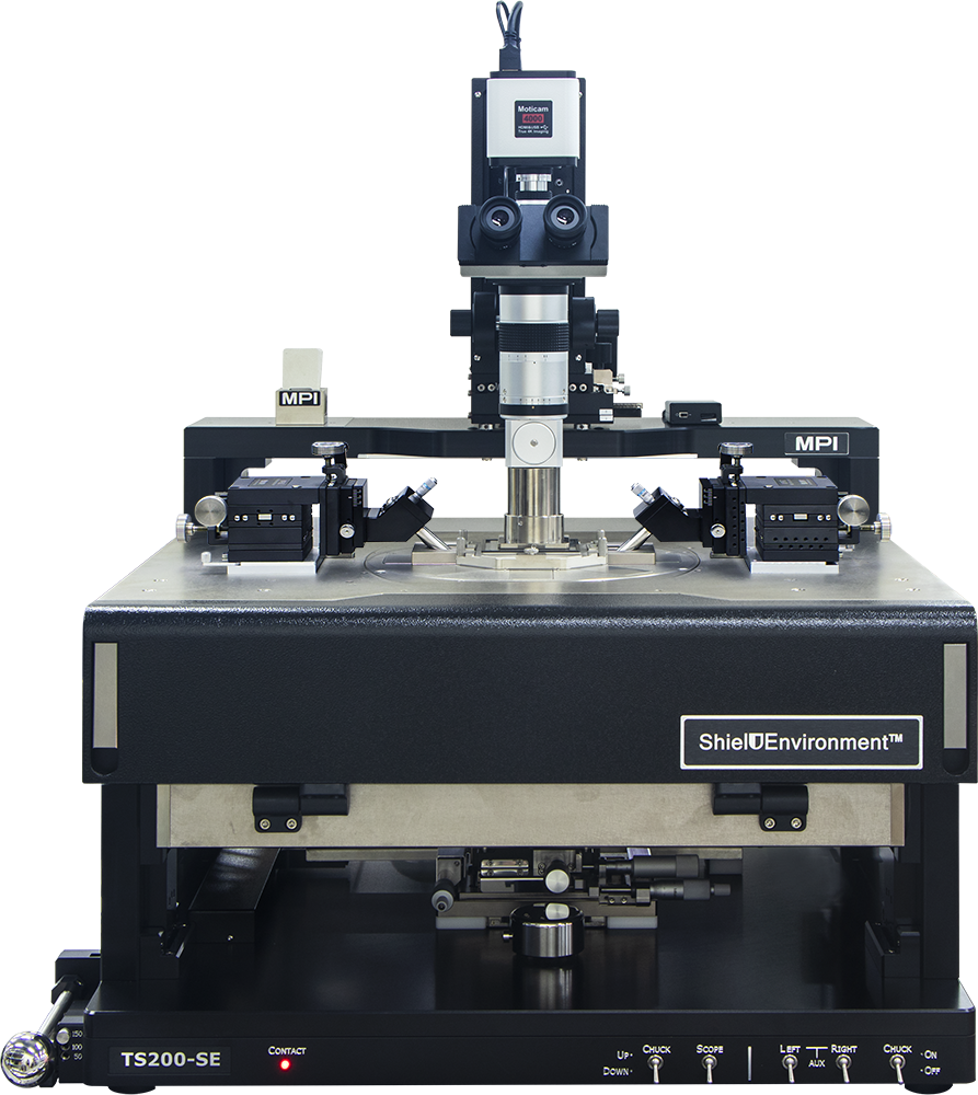
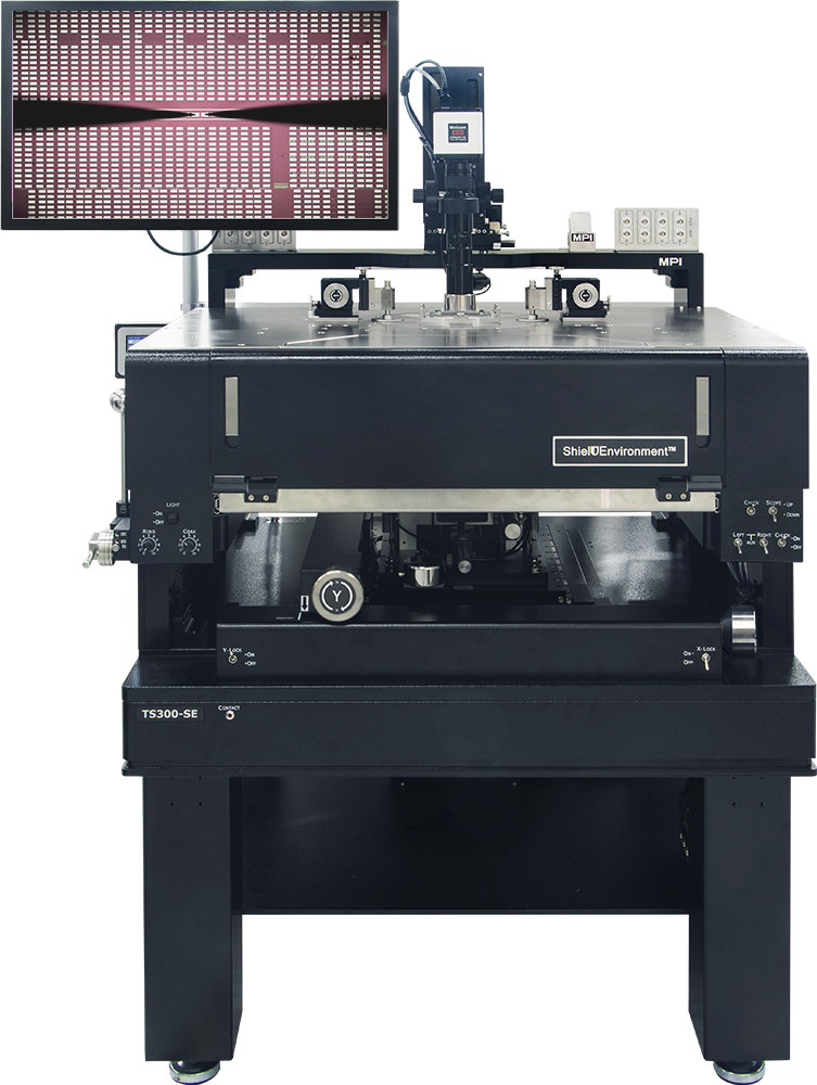
The MPI TS200-SE and TS300-SE probe system incorporate the ShielDEnvironment™ providing optimal EMI shielding which allows ultra-low noise device on-wafer measurements mainly for Device Characterization and Modeling applications.
The modular design concept of all MPI manual probe systems allows a unique upgrade path towards reduced cost of ownership.
TS200-SE

TS300-SE


TS2000-SE
TS3000
TS3000-SE
SiPH Probe System
TS2000
TS2000-IFE


TS150-HP & TS200-HP
TS2000-DP Probe System
TS2000-HP Probe System
TS3000-HP
TS3500-HP
TS2500-DP


TS3500-SE with WaferWallet®
TS2000-IFE with WaferWallet®MAX
TS2500 Series
TS2500-SE


Chuck Systems
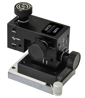
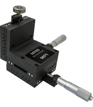
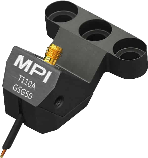
MicroPositioners
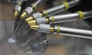
DC & RF Probe Arms
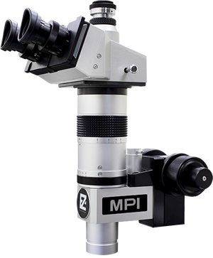
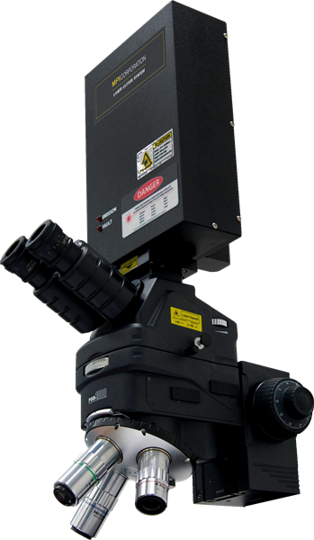
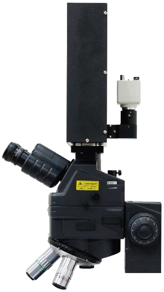
Optics
Laser Cutter
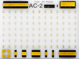
TITAN™ RF Probes
Calibration Substrates
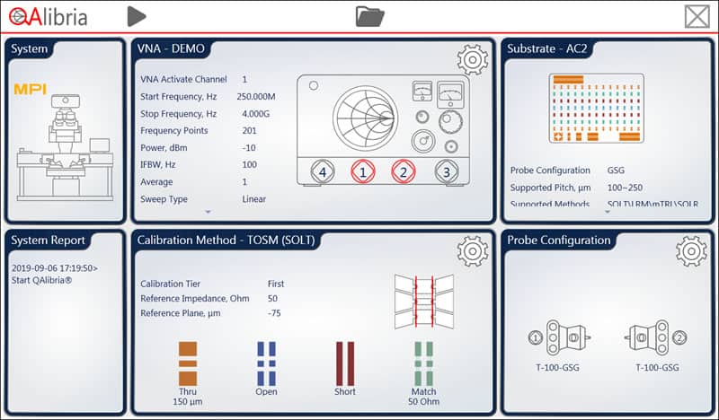
RF Calibration Software
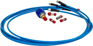
RF Accessories
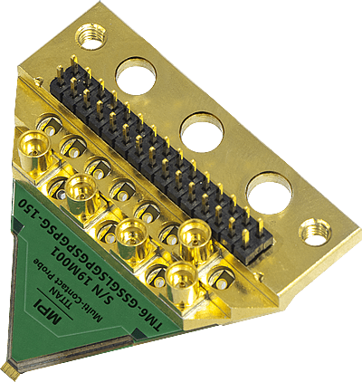
TITAN™ Multi-Contact Probes