
RF and mmW Applications


MPI Definition
Wafer level RF and mmW characterization is a critical part of RF and microwave IC’s development, design debug and modeling of modern high-performance semiconductor devices.
Due to the high complexity and specific requirements to the wafer-level integrations of the RF instrumentation such as VNA, frequency extenders, automated impedance tuners, couplers, Bias-Ts and many other system components, MPI pays a very special attention to this application segment targeting the best possible measurement accuracy.
Major Requirements
It includes small- and large-signal measurements, S-parameters, source and load pull impedance matching for RF power and RF noise characterization. These applications challenge the system for its high mechanical stability, shortest signal path, highest directivity of measurements, repeatable and consistent contact performance on various DUT pad metallization types and over time, as well as accurate system RF calibration down to the DUT terminals.
MPI Solutions
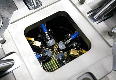
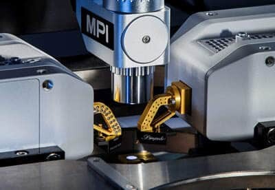
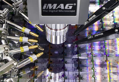
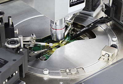
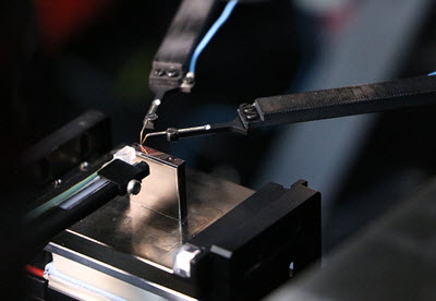
The rigid MPI Engineering Probe Systems are the ideal choice for RF and mmW measurement applications. The compact footprint ideally fits to the requirements of integration with complex RF power and Noise characterization systems. Accurate and back-lash free RF MicroPositioners provide precise positioning of the RF probes.
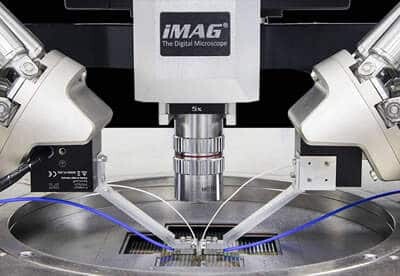
MPI explicitly designed and mmW dedicated, manual probe systems TS150-THZ, TS150-AIT & TS200-THZ, the high-end mm-wave MP80 MicroPositioner and the single-tube MPI SZ10 or MZ12 microscopes with unique combination of high magnification and long working distance Optics enable integrating the mmW, sub-mmW VNA frequency extenders and automated impedance tuners, closest possible to the DUT, for the shortest signal path and guaranteeing best possible measurement directivity and accuracy.
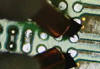
MPI TITAN™ RF Probe Series with its unique design and MEMS manufactured tips provide unique visibility, low resistance and high consistency of the contact even on hard to probe Aluminum pads.
Pioneering QAlibria®calibration software and verified Calibration Substrates realize industry-standard and advanced calibration methods, as well as the metrological-level RF calibration solutions.
MPI THZ-Selection option converts TS2000-IFE system into a dedicated, mmW and THz probe station, as the first one on the market, so that automated testing of 200mm wafers with unsurpassed measurement accuracy is possible now. Configurations with MPI motorized MicroPositioners are very common, in case of more measurement and calibration automation.
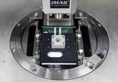
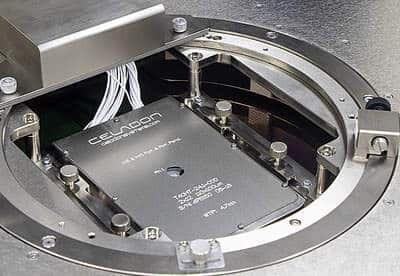
MPI TS2000, TS3000 and TS3500 are automated probe systems with minimized platen to DUT distance. Dedicated automated impedance tuner platen extensions are making these probe stations ideal platforms for load-pull measurements.
TS2500 is MPI’s 200 mm fully automatic probe system series, specifically developed to address Radio Frequency (RF) or High Power device testing at the production level. The system is designed for 24/7 production reliability and compatible with all MPI system accessories.