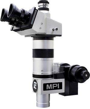
MPI RF Probes & Accessories
MPI RF Probes
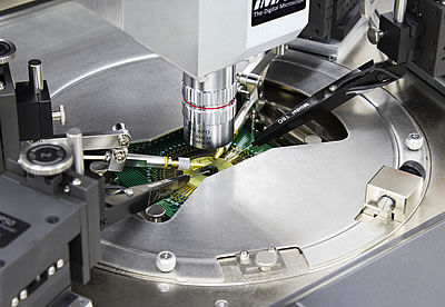
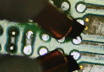
RF wafer probes convert the electro-magnetic energy traveling along the coaxial cables to the on-wafer DUT and its contact pads. The conversion has to be carried out with minimal distortions and energy loss.
There are significant differences between the various types of RF DUTs: from discrete elements to complex ICs operating at very wide frequency range. RF probe technology therefore must support a wide range of frequencies and pitches as well as the various tip configurations. Finally, the probe price together with the probe lifetime directly influences the DUT cost of test.
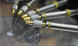
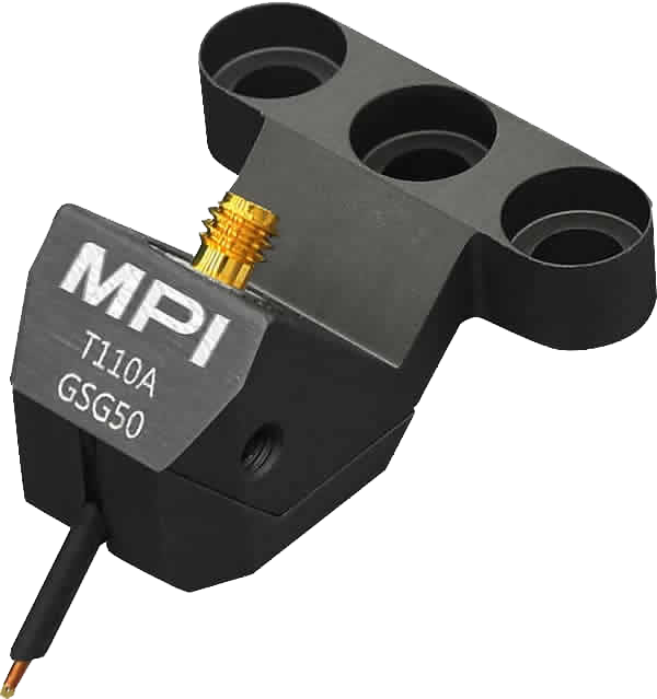
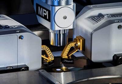
With a critical understanding of the numerous challenges associated with today’s RF applications, MPI Corporation has developed TITAN™ RF Probes, a product series specifically optimized for these complex applications centered upon the requirements of advanced RF customers. TITAN™ Probes provide the latest in technology and manufacturing advancements within the field of RF testing utilizing MPI’s proprietary world-class MEMS technology.

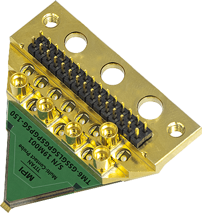
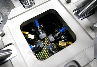
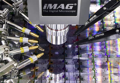
Multi-Contact Probes
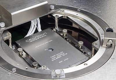
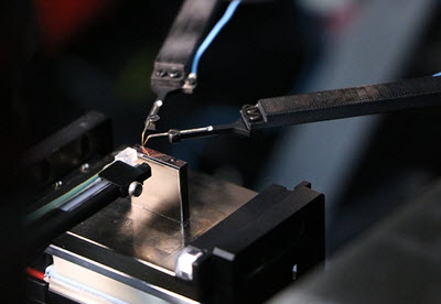
Design debug and test of the modern RF ICs is a task of another level of complexity. Along with the RF input and output signals, the device under requires oscillation-free bias as well as with the digital control signals (e.g. for changing gain of the amplifier). All these needs to be delivered to the IC over the smallest possible contact pads, individually configured for each product. The Multi-Contact Probe expands MPI proprietary TITAN™ RF probing technology to serve these test needs. Featuring up to 15 contacts with RF bandwidth of up to 6 GHz each and the pitch ranging from 50 to 300 μm, this probe is individual configurable to match your specific requirements. It is built using standard off-the-shelf components and thus has the shortes lead time. You can start test your RF IC just in one week after you configured your TITAN™ Multi-Contact Probe using online design capture tool.

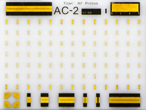
Calibration Substrates
Commercial probe-tip RF calibration standards are made in coplanar design and include calibration elements of different kinds: open, short, load, and lines. Accordingly, various types of probe tip calibration can be carried out.
MPI AC-series of calibration substrates are specially developed to provide accurate probe tip calibration of TITAN™ Probes. The design of calibration standards is matched with the probe configuration and the pitch size. The model parameters for standard equivalent impedances define the accuracy of calibration. That is why they were extracted with highest precision.

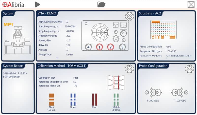
RF Calibration Software
MPI’s long-time experience in wafer-level RF calibration and a detailed understanding of the microwave measurement specifics are at the bottom of QAlibria®– MPI’s RF calibration software.
QAlibria® is designed to make complex and tedious task of RF system calibration simple. Its unique features of the multi-touch and multi-language graphical user interface as well as the original NIST multi-line TRL calibration capability revolutionized the wafer-level RF system calibration.

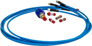
RF Cables and Accessories
The success of the RF measurements depends on the optimal configuration of the entire system. To reach the best in class system performance, MPI offers an excellent selection of flexible cables, waveguide sections, as well as a wide range of adapters for complete RF probe system integration. Calibrated torque wrenches, TITAN™ probe planarization and cleaning accessories help for the keep the system measurement performance at the highest level for long time.


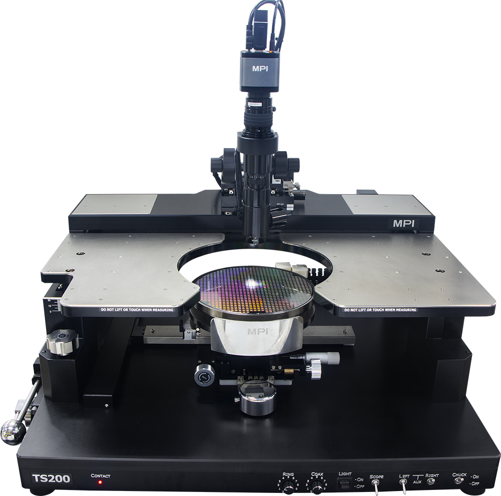
TS200
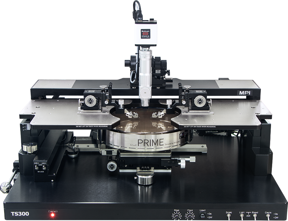
TS300
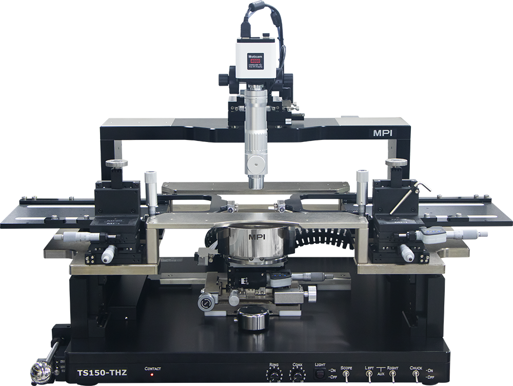
TS150-THZ
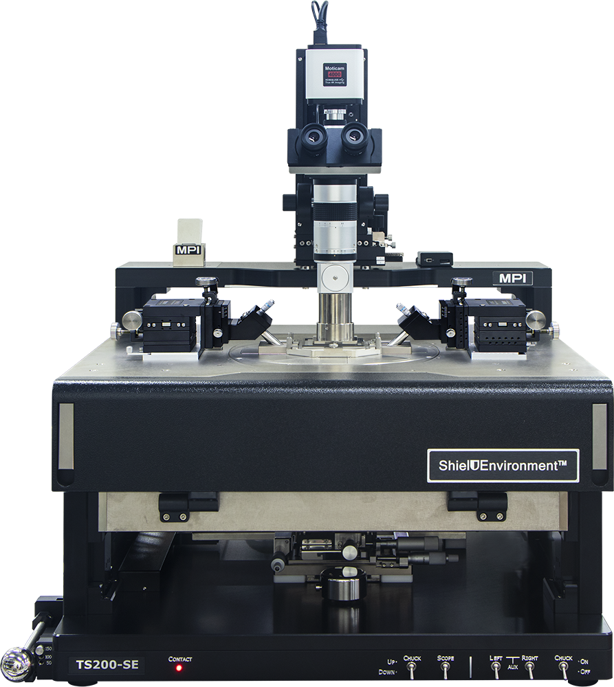
TS200-SE
TS150
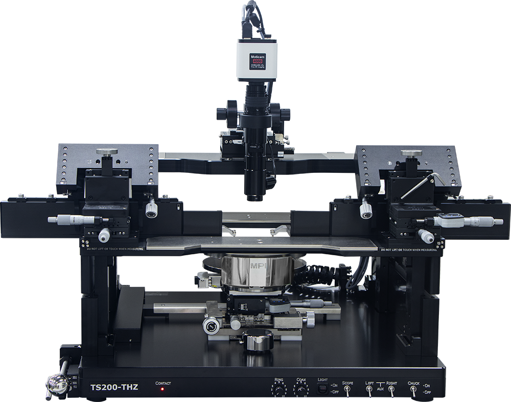
TS200-THZ
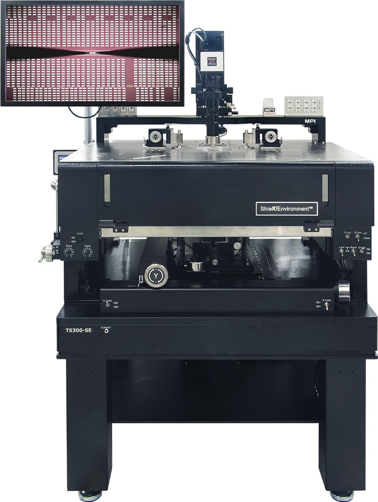
TS300-SE