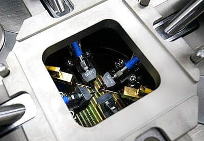
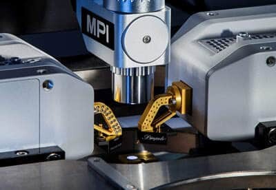
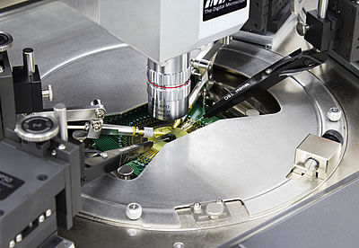
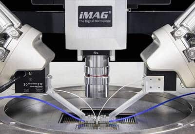
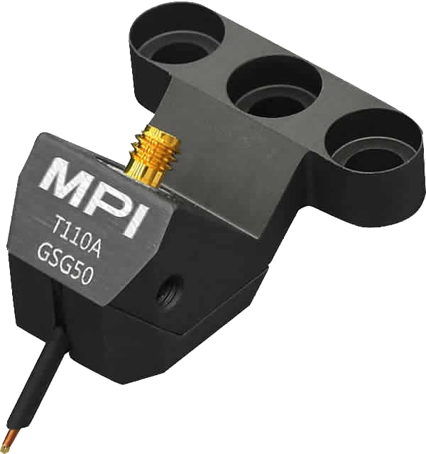
TITAN™ Multi-Contact Probes

MPI TITAN™ Multi-Contact Probe

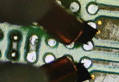
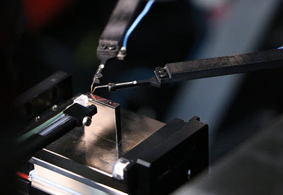
The Multi-Contact Probe expands MPI proprietary TITAN™ RF probing technology for characterization of RF ICs. Featuring up to 15 contacts with RF bandwidth of up to 6 GHz each and the pitch ranging from 50 to 300 μm, this probe is fully configurable for your test needs.

Use Online Design Capture Form to build your probe by choosing RF signal (S), logic (L) and power supply (P) channels according to your IC pad layout.
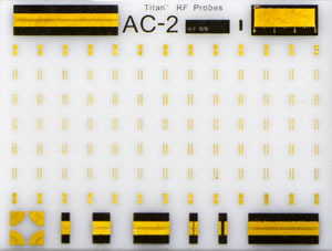
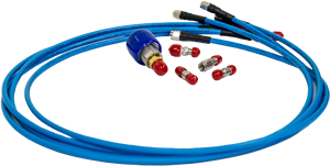
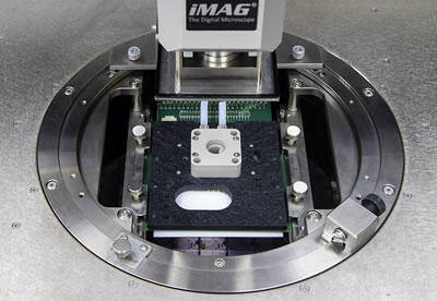
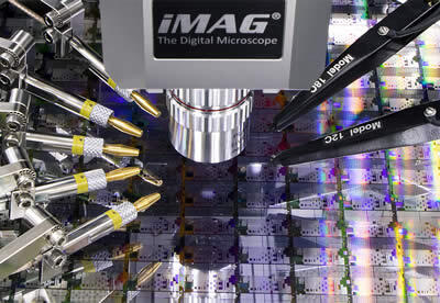
Features & Benefits

Modularity & Fast Delivery

The Multi-Contact Probe can be individual configured by using a modular design, pre-standardized components and MPI own MEMS based probe tip technology, which allows fast delivery, typical within five working days. This probe provides you with the fastest time-to-data of your IC with its just one week lead time.

Cutting-Edge Design: 50 μm Pitch, Over 1 Million Touchdowns, Compact

TITAN™ Multi-Contact Probe is the shortest configurable probe. It enables a wide temperature range characterization of the large IC and is more convenient to use in shielded environment. It is fully compatible in size with standard RF probes and thus it allows quadrant test configurations without further re-adjustments.

TITAN™ Multi-Contact Probe was designed to reduce the cost of test of modern highly-integrated RF ICs. It offers a unique combination of the contact width of 20 μm with the smallest probe pitch (starting from 50 μm),  longest lifespan (over 1 million touchdown cycles on Al pads), affordable price and short lead time.

MPI TITAN™ Multi-Contact Probe

TITAN™ Probe MEMS Tip Technology

TITAN™ Multi-Contact Probe incorporates MEMS contact tips with tightly controlled impedances. They ensure highly repeatable calibration and measurement results as well as uniformed contacting characteristic over a wide temperature range and unmatched number of contact cycles. 

MPI TITAN™ Multi-Contact Probe - MEMS Technology

Unique Contact Structure

Like any other MPI RF probes, TITAN™ Multi-Contact Probe delivers excellent and real time visibility of the tip contacts due to the unique protrusion tip design. For the first time, highly accurate positioning of the probe on IC’s pads became possible even for unexperienced operators.

Field Application Engineer

Job Location: San Jose, CA

Job Duties:

  • Assist in developing HW and SW measurement methodologies/solutions for analytical wafer probe solutions with signal applications from DC to millimeter wave frequencies as well as Silicon Photonics (SiPH);
  • Collaborate with customers on their measurement challenges, and provide applications specific product training;
  • Provide pre- and post-sale support to AST, customers, service department, and the sales channel developing HW and SW measurement solutions for analytical wafer probe stations;
  • Define application-specific solutions based on customer-provided device data and facilitate both customer and divisional teams to successful results;
  • Perform product training seminars for customer and sales channels as well as participate in trade shows and technical seminars;
  • Make recommendations regarding product improvement, new products, and quality enhancement;
  • Author, document, publish, and present measurement solutions via Seminars, Applications Notes, Briefs, and White Papers;
  • Prepare, plan, and assist with customer product demonstrations that highlight value-based differentiation of AST product offerings;
  • Develop unique and individual customer presentations designed to professionally position the MPI brand in the North American market and deliver formal presentations to customers.

Job Requirements:

Master’s degree in Electrical Eng., Electronics Eng., Physics, or Photonics; Must possess 6 months of relevant work experience; Travel to customers’ sites in US and headquarters in Taiwan is required.

Send resume to: MPI America, Inc., 2360 Qume Drive, Suite C, San Jose, CA 95131, Attn: Janet Chiang