
Failure Analysis (FA)

MPI Definition
Root cause identification of failing devices (e.g. field returns or new designs) is essential for all semiconductor manufacturers and design houses.
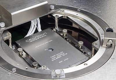
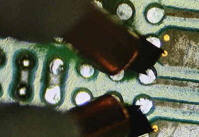
Especially complex failure analysis such as failure of open/floating signal net in IC devices is done by electrical micro-probing measurements by net signal tracing. Upon failure localization requires focused ion beam (FIB) depositing of so called “mini-pads” (e.g. 5 x 5 µm).
Failure localization with typical hot spot and emission analysis is another appropriate method for defect identification.
The physical failure analysis based on submicron probing or on SEM, TEM, EDX, AFM tools is not part of MPI consideration.
Major Requirements
There are several major fragments in this process:
-
-
- Verification of electrical and functional failures based on leakage or simple open/short measurements.
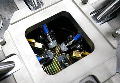
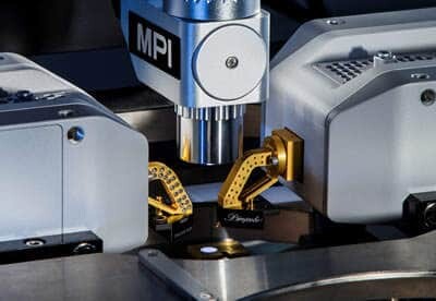
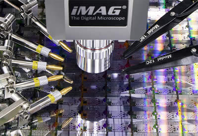
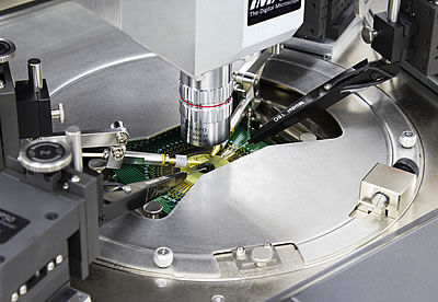
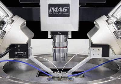
- Micro-probing internal nodes on “mini pads” using high-impedance Picoprobes.
- Navigating to the “mini pads” (which can number in the thousands within complex ICs) is a significant challenge.
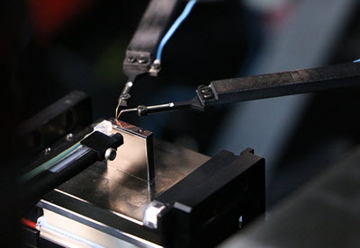
- The IC is powered via a probe card, and micro-probing must be performed simultaneously with several single probes.
- These probe cards are often customized and are typically very long (>13”), containing active components near the DUT (Device Under Test).
- Failure localization is carried out using standard techniques like hot spot and emission analysis.
- Laser cutting is used to open passivation layers or cut metallization lines.
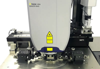
- Micro-motion analysis is performed at the wafer level, particularly for MEMS devices.
- A 10 kV test environment is necessary for failure analysis on high-power devices.
- High optical resolving power optics are required for this type of work.
-
MPI Solutions
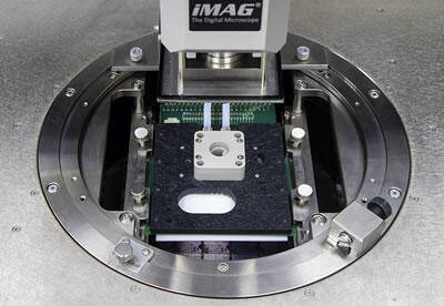
MPI Test Solutions for FA applications come with everything needed to achieve accurate measurement results in the shortest time, with maximum confidence. The highly stable Engineering Probe Systems and highly accurate MicroPositioners provides best solution for electrical failure verification, localization and debugging. With the vibration isolated environment and wide zoom & high magnification microscopes provide the ability to probe the structure as small as one micron.
MPI TS3000 probe systems, offer uniquely the simultaneous use of probe card and MicroPositioners (DUT driving & internal signal measurements), especially at temperatures down to negative 60°C.
The low platen to chuck distance makes the Picoprobing very convenient.
The unique MPI Laser Cutter System LCS-635 is designed for accurate and reliable Failure Analysis and variable configurations based on 1064 nm, 532 nm, 355 nm or 266 nm wavelengths provides the capability to remove several semiconductor materials and metals selectively.
MPI Engineering Probe Systems are easily configured with emission microscopes such as from Hamamatsu Photonics Japan to detect and localize the IC failures. In addition, the TS150/TS200-HP probe systems are the ideal choice for the equivalent analysis of High Power devices up to 10 kV and 600 A.