MPI LED Mapping Sorter Series

blank
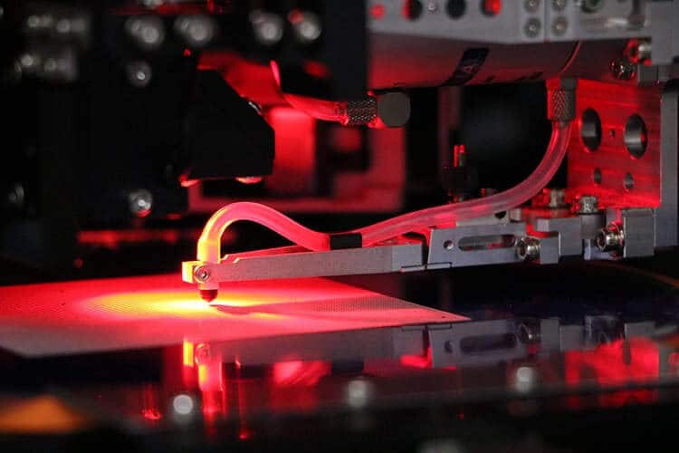
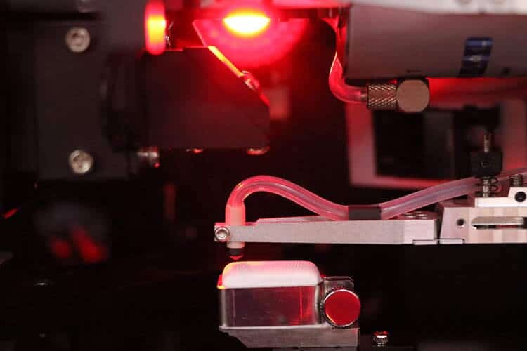
MPI proudly presents the LED Mapping Sorter Series designed using a modular architecture with unsurpassed flexibility allowing every system to meeting each customer’s precise requirements. Utilizing advanced Pick & Place sorting process technology, the MPI LED Mapping Sorters deliver high speed die sorting cycle times of 55msec/chip or less. The Mapping Sorter series feature extra-large sorting area (8”) and bin area (140mm X 140mm) with a unique four-sorting arm design enhancing both the production efficiency and high-volume throughput.


MPI’s best-in-class engineering teams work collaboratively with many organizations to provide tailor-made and turnkey solutions. This ensures unsurpassed innovation further supporting customer’s competitiveness in their respective markets.

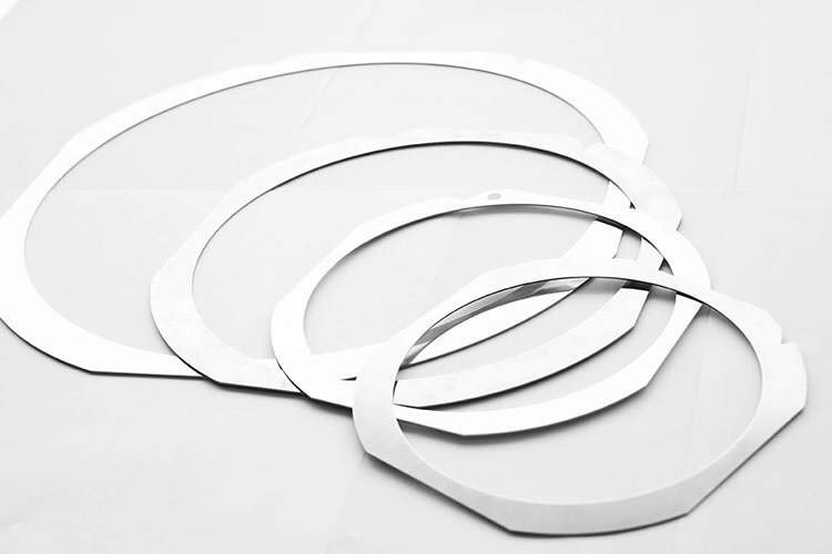
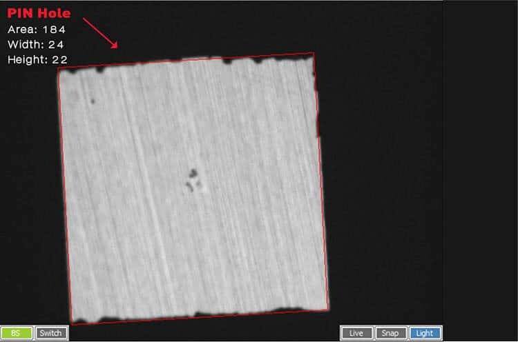
MPI LED Mapping Sorter Series easily accommodate various input/output carrier types. MPI’s Mapping Sorters can be optionally configured with Back Side Inspection (BSI) bringing production yields to a whole new level. Delivering the highest accuracy and reliability, MPI LED Mapping Sorters are ideal for vertical chip, CSP, GaN, GaAs, Vertical LED, Flip Chip, and Laser Diode test and sort applications.

Features & Benefits

Unbeatable Production Efficiency

Equipped with a unique four-sorting arm design and driven by the ultra-fast linear motors, the MPI LED Mapping Sorter facilitates high speed die sorting with record cycle times reaching 55msec/chip and superior Pick & Place accuracy of +/- 20μm.

Versatile Carrier Handling Support

MPI LED Mapping Sorters are capable of handling dies as small as 0.15mm to 2mm with various flexible input/output carriers.

Up to 200 Bin Frames

MPI LED Mapping Sorters are optimized with many automation features that help eliminate processing errors, operator intervention and downtime. The results are higher productivity, greater reliability, and better uptime ratios. System automation features include:

  • Auto-Clean Nozzle
  • Auto-Teach Pick Level (ejector & nozzle)
  • Semi Auto Nozzle Center Alignment
  • Auto-Teach and easy Change-over between different materials
  • Auto-Prevent Wafer Dislocations

Intelligent Software Algorithm

Configurable up to 10 cassettes enables the Sorter Systems to support 200 bin frames. The smart software algorithm allows user designation of each cassette/frame (input, output, wafer, buffer, fully, empty) according to your application and process requirements.

Back Side Inspection (BSI)

Production yields can be further enhanced by using the optional Back Side Inspection (BSI) module. Throughout the entire sorting process, the BSI module detects the defects (e.g., probe mark, crack, double-die, fracture) on the back side of the LED chip. The inspection raw data is recorded via MPI self-developed software that monitors the defect trends and thereby reducing production abnormalities for optimal production quality.

Easy-to-use Software

*Design, feature, and specifications listed herein may vary according to individual equipment configurations. NOT all specifications are valid simultaneously. These will be spelled out once systems are configured for your exact application.

The powerful MPI self-developed control software features straightforward operation and intuitive on-screen navigation. MPI LED Sorters are compliant with industry standard SECS/GEM communication interface protocols.

EXPLORE MPI PHOTONIC APPLICATIONS

MPI offers a comprehensive portfolio of test, measurement and inspection solutions meeting the demands of the Photonics, Optoelectronics, Semiconductor, and Laser industries.

MPI Photonic solutions for Optical Communication applications (Datacom, Telecom, Laser, Photodetector, Photodiode)

OPTICAL COMMUNICATIONS

Precision test and measurement solution for optical devices such as Photo Detectors and Laser Diodes

MPI Photonic solutions for Optical Sensing applications (VCSEL, LiDAR, ToF, Time-of-Flight, 3D Sensing, Facial Recognition, Automotive sensing)

OPTICAL SENSING

Turn-key solution addressing 3D sensing consumer (Facial Recognition, Gesture Recognition, AR) and Automotive (LiDAR) applications

MPI Photonic solutions for Micro Display applications (Micro LED, Mass Transfer, VR, AR)

MICRO DISPLAY

Accurate probing tool combined with idea mass transfer method

MPI Photonic solutions for LED applications (Automotive / General Lighting)

LED

Complete solution covers testing, sorting, and inspection from wafer to package die level

MPI Photonic solutions for Optical Sensing applications (VCSEL, LiDAR, ToF, Time-of-Flight, 3D Sensing, Facial Recognition, Automotive sensing)

SILICON PHOTONICS

Dedicated SiPH on-wafer tests designed to perform repeatable low noise measurements

Need help or have questions?

Field Application Engineer

Job Location: San Jose, CA

Job Duties:

  • Assist in developing HW and SW measurement methodologies/solutions for analytical wafer probe solutions with signal applications from DC to millimeter wave frequencies as well as Silicon Photonics (SiPH);
  • Collaborate with customers on their measurement challenges, and provide applications specific product training;
  • Provide pre- and post-sale support to AST, customers, service department, and the sales channel developing HW and SW measurement solutions for analytical wafer probe stations;
  • Define application-specific solutions based on customer-provided device data and facilitate both customer and divisional teams to successful results;
  • Perform product training seminars for customer and sales channels as well as participate in trade shows and technical seminars;
  • Make recommendations regarding product improvement, new products, and quality enhancement;
  • Author, document, publish, and present measurement solutions via Seminars, Applications Notes, Briefs, and White Papers;
  • Prepare, plan, and assist with customer product demonstrations that highlight value-based differentiation of AST product offerings;
  • Develop unique and individual customer presentations designed to professionally position the MPI brand in the North American market and deliver formal presentations to customers.

Job Requirements:

Master’s degree in Electrical Eng., Electronics Eng., Physics, or Photonics; Must possess 6 months of relevant work experience; Travel to customers’ sites in US and headquarters in Taiwan is required.

Send resume to: MPI America, Inc., 2360 Qume Drive, Suite C, San Jose, CA 95131, Attn: Janet Chiang