
Optical Sensing
OPTICAL SENSING TEST SOLUTIONS
Vertical Cavity Surface Emitting Laser (VCSEL) based optical sensing technologies are finding their way into numerous consumer (Facial Recognition, Gesture Sensing, Augmented Reality) and automotive (LiDAR and In-Cabin Monitoring) applications. MPI’s comprehensive portfolio of test and measurement solutions are ready to meet the demands of the VCSEL based optical sensing market.
MPI’s array of optical sensing solutions are well suited for the demands of both production and engineering environments. We are ready to meet customer’s critical testing and back-end processing needs:
-
- Parametric Test and Measurement
- Material Handling
- Inspection
- Wafer Level Reliability Test / Wafer Level Burn-in (WLBI)
MPI optical sensing solutions have been designed to meet the entire spectrum of VCSEL designs and configurations.
-
- Front Emitting VCSEL
- Rear Emitting VCSEL (Flip-Chip)
- Wafer, Package, & Die Level
THE TECHNOLOGY
The Light-Current-Voltage (LIV) sweep test is a fundamental optical measurement used to determine the operating characteristics of devices such as laser diodes (LDs) and VCSELs.
MPI specializes in integrating a variety of Source and Measurement Units (SMU) providing accurate and synchronized power and voltage measurements in both pulsed (mS to nS) and CW modes.
-
- High speed nanosecond test instrumentation capability
- Electrical, Mechanical & Thermal system design to minimize the effects of self-heating, contact resistance and parasitics
- High speed optical measurements using integrating spheres for both low and high power VCSELs

Pulse Width at 10µs

Pulse Width from 10µs to 500µs
High Speed Pulsed Optical Measurements
-
- Laser Diode Driver Integration for LiDAR / Time of Flight (TOF) applications
- High fidelity current stimulus control enabled by MPI’s high frequency probe card technologies
- Synchronized electrical/optical measurements and data capture
- Interleaved current pulse generation for enhanced high throughput testing
Optical Spectrum Measurements
Spectral measurement & analysis over a broad range of temperatures.

Spectrum Measurement

-40°C ~ 125°C Measurement Capability

Laser Characterization
Laser Characterization
Laser Electrical / Optical performance characterization
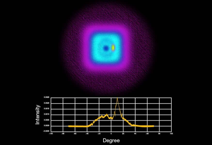
Far Field Measurements are used to characterize a VCSEL Array’s optical profile at longer working distances.
MPI specializes in:
-
- Optical system design and integration to achieve high quality Far Field images with working distances ranging from 4mm to 1.5m or more
- Typical Far Field optical measurements include:
-
- Divergence Angle
- Eye Safety
- Uniformity
- Efficiency
-
- Both Panel and Direct measurement methodologies are supported
")
VCSEL Array
(Far Field Measurement)
")
VCSEL Array with Lens Attached
(Far Field Measurement)
Far Field Measurement Options
Far Field measurement examples of different device types
Eye Safety Measurement
Integrated analysis software for eye safety calculations
Laser Eye Safety Calculation

Direct Camera Far Field Measurement
")
Far Field Light Collection Structure
(Panel with Direct Camera)
Far Field Measurement Options
Two Far Field measurement options are available for specific optical device test requirements
Near Field measurements are used to characterize the optical power and beam characteristics in VCSEL arrays on a per emitter basis.
MPI specializes in:
-
-
- Optical system design and integration to achieve high quality Near Field measurements for VCSELs with emitting apertures ranging from 5µm to 20µm
- VCSEL array characterization (Uniformity, Detection of faulty emitters and pass/fail grading)
- Optical Beam Characterization:
-
-
- Numerical Aperture (NA)
- Beam Diameter [D4σ (D4Sigma), D86]
- Beam Quality (M2) using sequenced near field imaging
-
-
- High speed optical measurements
-

Near Field Emitter Characterization

Near Field Single Emitter
VCSEL Near Field Emitter Characterization
VCSEL Array NF measurements on a per emitter basis for all standard parameters
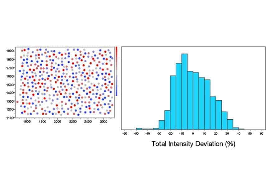
VCSEL Array Parametric Distributions
Examples of VCSEL array intensity and beam diameter distributions
Near Field Intensity Measurement
")
Near Field Beam Diameter
(D4Sigma, D86)
 Measurement")
Near Field M2 (M-Squared) Measurement
Near Field M2 Measurement
Near Field M2 measurement using sequenced near field images
MPI’s portfolio of automated test and material handling solutions readily meet the diverse needs of the optical sensing manufacturing market. Whether it be thin wafer handling, device pick and place (PnP), extreme temperature testing or production data management, MPI has a solution that will streamline your production flow and enhance product yields.
MPI specializes in:
-
- Thin wafer handling solutions (Non-contact Bernoulli handler, Gel-Pak, and Carrier methods)
Extreme temperature testing:
-
- Wafer Test: -60°C to ~200°C
- Device Test: 0°C to 100°C
-
- Production test automation and data management
-
- Flexible recipe setting with multiple test sequence support
- Multi-die test support
- Configuration and test data management tools
-
- Thin wafer handling solutions (Non-contact Bernoulli handler, Gel-Pak, and Carrier methods)

Thin Wafer Handling - Gel-Pak
*Gel-Pak® is a Registered Trademark of Gel-Pak®, a Division of Delphon Industries.

Thin Wafer Handling-Non Contact Bernoulli Handler

Thin Wafer Handling – Carrier
Thin Wafer Handling Technology
Multiple thin wafer handling solutions available for different device types and manufacturing flows
Fully Automated Material Handling Capability
MPI has a complete line of die probers/sorters featuring highly reliable and precise pick and place mechanics suitable for a wide variety of high throughput applications

Die Pick and Place
 Pick and Place")
Package (EEL) Pick and Place

Thermal Chuck for Wafer Testing
*Image Courtesy of ERS electronic GmbH

Thermal Chuck for Single Device Testing
Thermal Control
Various thermal chuck options for Wafer/Die level testing
-
- Wafer Testing: -60ºC ~200ºC
- Single Device Testing: 0ºC to 100ºC

Multiple Recipe Settings
Easy-to-use Software Suite
MPI’s powerful control software combines highly efficient operation with an intuitive and easy-to-use interface
-
- Flexible recipe setup enables smooth and efficient operation per customer defined test plans
- Multi-die probing capability boosting production throughput enabling lower cost of test
THE BENEFITS
Superior Optical Expertise and System Integration Capability for Customer’s Requiring High Volume Manufacturing, Development and Test of Laser Diodes
![]()
-
-
- High precision test and measurement results
-
![]()
-
-
- High quality probing with optimizing automation
-
![]()
-
-
- Proactive service and training support to keep your equipment running with minimal interruptions
-
![]()
-
-
- Controlling all aspects of mechanical/electrical device contact
-
![]()
-
-
- Customer-centric customizable solutions for your specific requirements
-
EXPLORE MORE MPI PHOTONIC SOLUTIONS

OPTICAL COMMUNICATIONS
Precision test and measurement solution for optical devices such as Photo Detectors and Laser Diodes

SILICON PHOTONICS
Dedicated SiPH on-wafer tests designed to perform repeatable low noise measurements


LED
Complete solution covers testing, sorting, and inspection from wafer to package die level
Need help or have questions?