Reliable & reproducible
Designed by an experienced R&D team, our ISO-certified test systems ensure consistent, high quality, and accurate results.
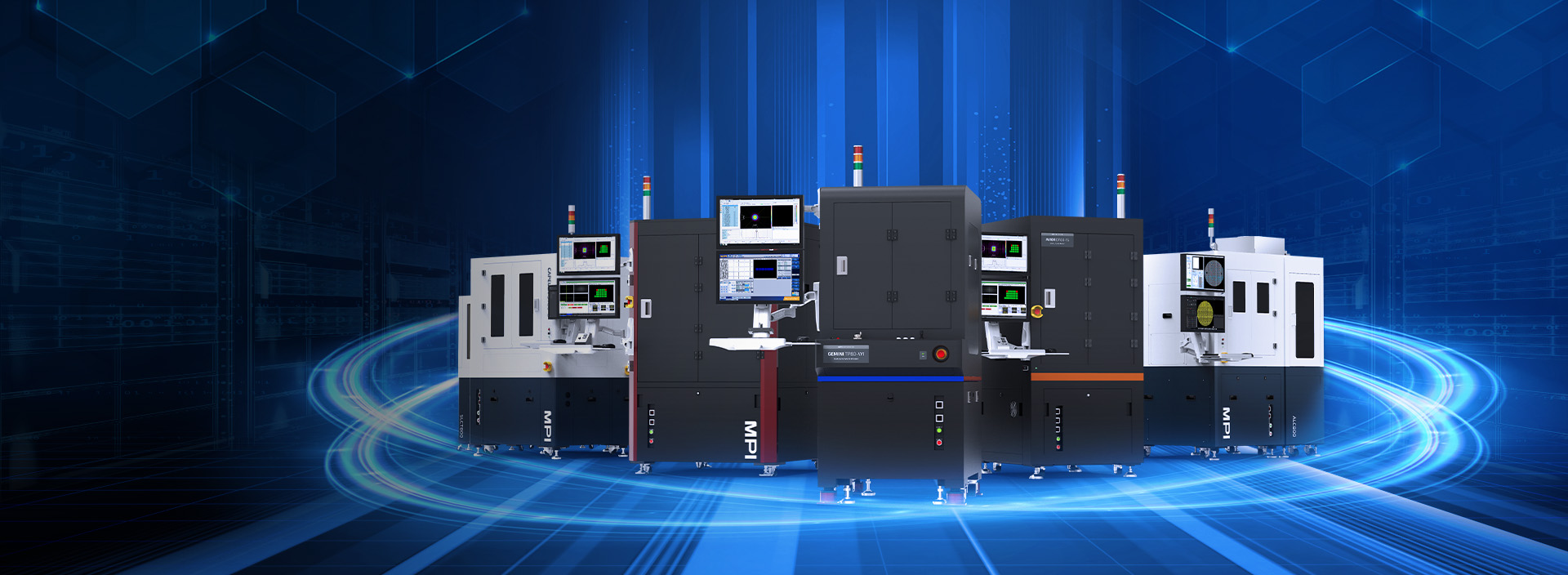
Universal control software
All MPI PA test systems can be controlled directly using the MPI SIRIUS software suite.
Future-proof
The scalable structure enhances overall cost efficiency, long-term competitiveness, and responsiveness to market dynamics.
Comprehensive support
Ensuring your system’s uptime is our top priority. We offer support via online, phone, email, remote connectivity, and onsite service, giving you direct access to MPI PA technical experts to address any issues promptly.
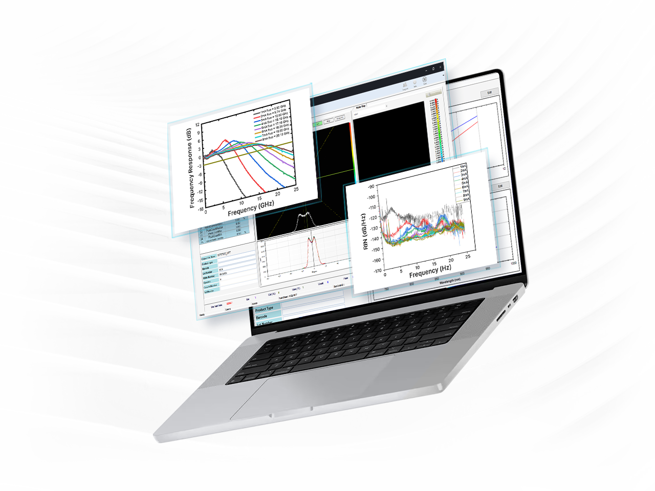
Precision test results
Easily generate precision test results using MPI STARGAZER photonics test system.
Extensive range of accessories
Enhance your system’s performance with a wide range of accessories and instrument integration options.
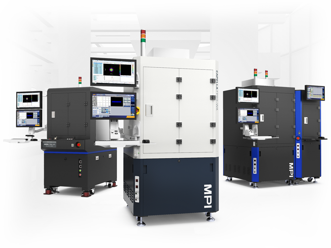
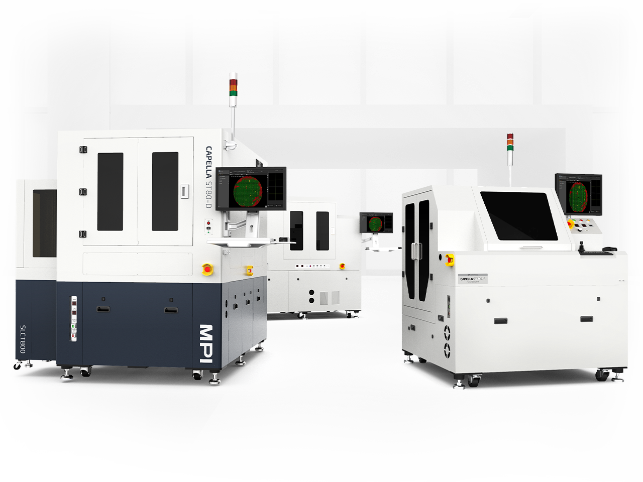
Wafer probing
Topside Probers / Flip-Chip Probers
Our comprehensive and highly automated wafer probing solution for testing photonic devices covers Laser Diodes, Photo Diodes, Micro LEDs, LEDs, and more.
Learn MoreDie probing
Die / Packaged Device Probers
Ideal testing platform design for singulated devices, including LED, LED CSP, VCSEL module, Edge Emitting Laser, edge coupling optical DUT, SiPh packaged device, power device, and more.
Learn More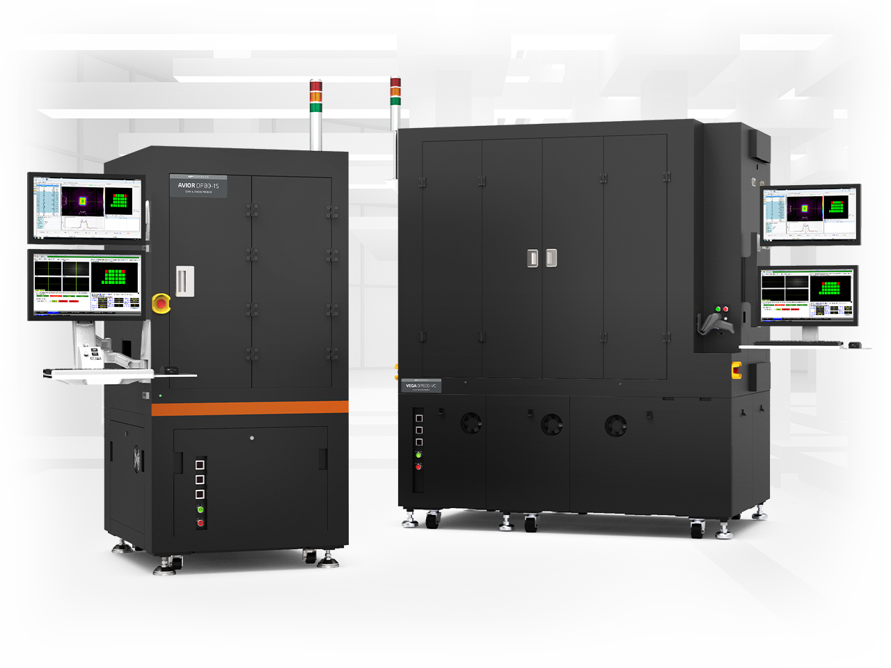
Die sorting
Die Sorters
Whether you require a high-speed die sorter for mass volume production or a single wafer prototype for research purposes, we have the right solution for you.
Learn MoreSeamless integration
Testing Solutions
Unlock the full potential of your testing with the STARGAZER Series Photonics Test System. Built on a modular software architecture, STARGAZER is designed for easy configuration and seamless integration to suit your specific testing requirements.
Learn More