


STARGAZER Photonic Device Test Solution
Seamless integration to unlock the full potential of your testing


Unlock the full potential of your testing with the STARGAZER Series Photonics Test System. Built on a modular software architecture, STARGAZER is designed for easy configuration and seamless integration to suit your specific testing requirements.
STARGAZER supports a wide range of photonics devices—from Sensing Lasers and Datacom Lasers to Photo Diodes, Micro LEDs, and more—delivering the versatility you need. Our system, integrated with high-quality measurement instruments from industry-leading partners, ensures precise and high-performance testing.
Simplify and streamline your testing process with STARGAZER. Get reliable and accurate results everyday. Start now and take your testing to the next level.
Sequence Control
Flexibly select and edit test sequence & parameters
Production Report
Manage lab / production recipe with ease via the intuitive software graphical user interface.
Recipe Management
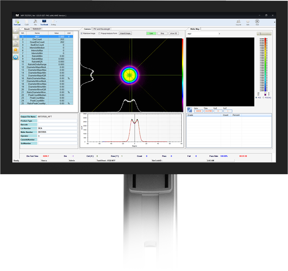
Real-time test results for DUT characterization and a comprehensive wafer report
Seamless Integration
With selected top third party measurement instruments through trusted partners to meet your specific test needs.


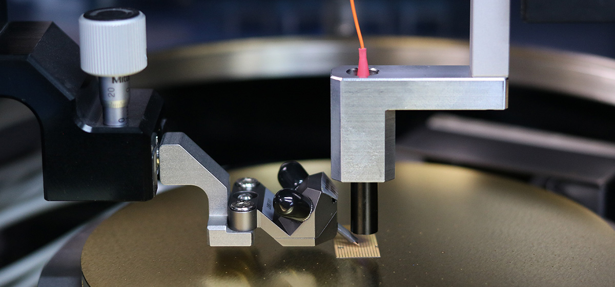
Sensing Laser Test and Measurement
STARGAZER LD200-S
| Key Feature |
|---|
|
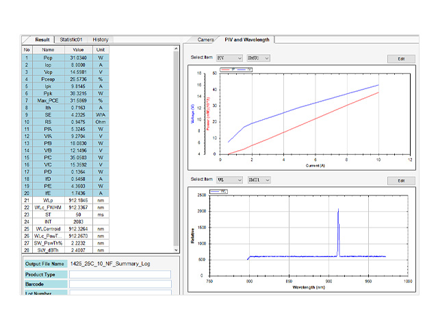
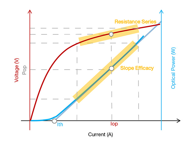
Current Control Real-time current and voltage measurement Integration of SMU, power meter, and Driver IC |
|
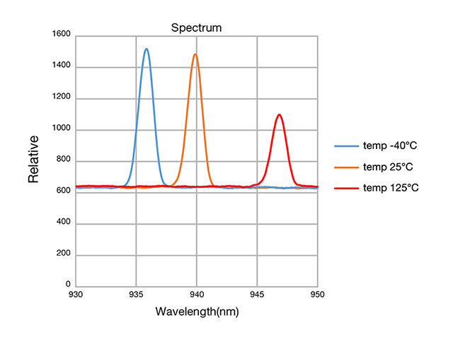
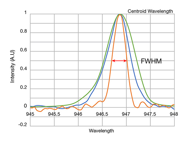
Spectrum Measurement Precise spectrum measuremen Integration of spectrum analyzer or spectrometer |
|
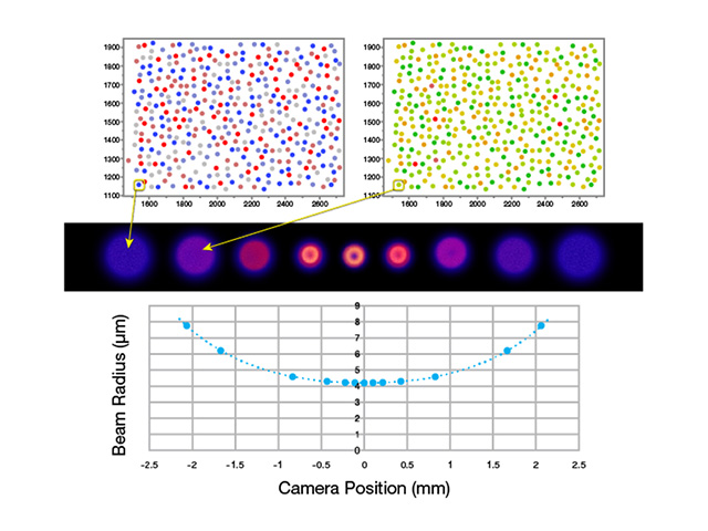
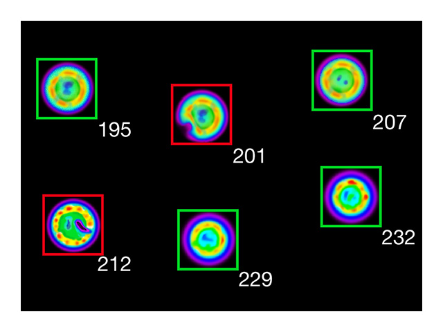
Near Field Pattern (NFP) / M² Characterization Near Field (NF) optics with large Field-of-view (FOV) Analytical tool for assessing NFP beam quality |
|
Far Field Pattern (FFP) Characterization FF optics for visible, NIR, and IR light ranges Analytical tool for evaluating FFP beam quality |
Datacom Laser Test and Measurement
STARGAZER LD200-D
| Key Feature |
|---|
|
Current / Bias Control Integration of SMU and power meter |
|
LIV / Spectrum Measurement Current / voltage measurement using meter Integration of spectrum analyzer or spectrometer |
|
Near Field Pattern (NFP) / Far Field Pattern (FFP) Characterization Integration of NF / FF optics Analytical tool for beam quality calculation |
|
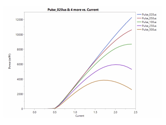
High-speed Device Characterization S-parameter characterization using RF probe and optical VNA Test instrument integration for Relative Intensity Noise (RIN) and Bit Error Rate (BER) testing |
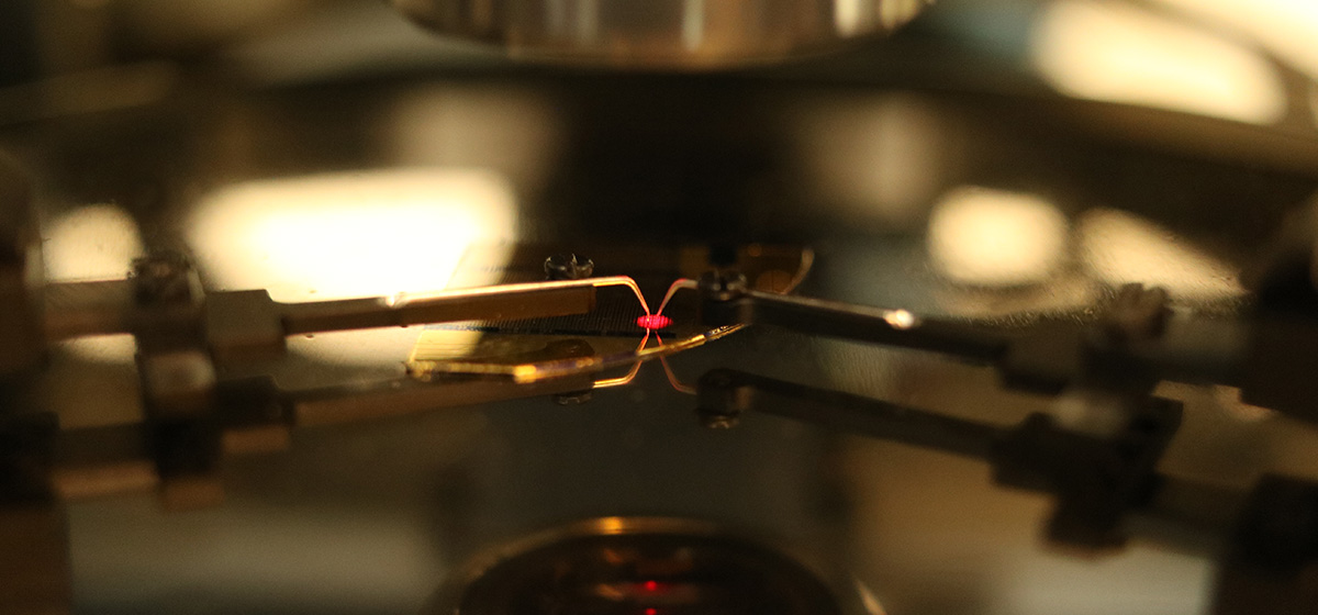
Photo Diode Test and Measurement
STARGAZER PD200
| Key Feature |
|---|
|
IV Sweeping Dark Current / Photo Current measuremen SMU integration for testing singulated / multi DUT |
|
Responsivity Illumination source control / Optical switch / Attenuator control |
|
Capacitance LCR measurement integration |
|
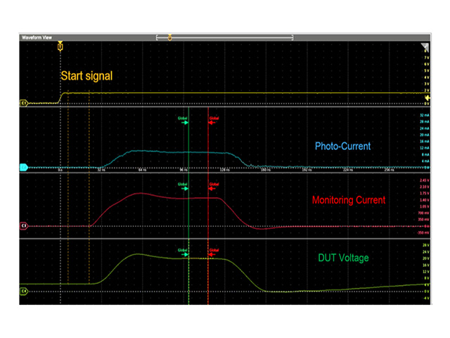
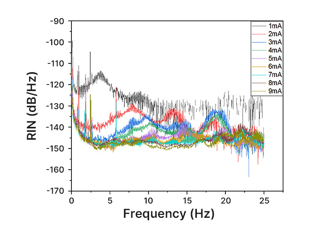
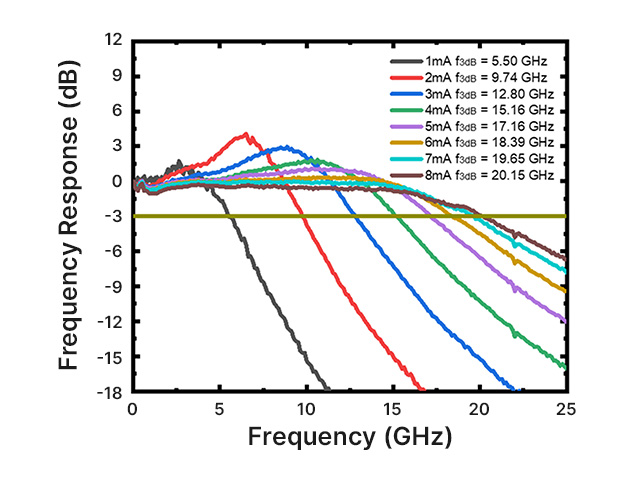
High-speed Device Characterization S-parameter characterization using RF probe and optical VNA Test instrument integration for Relative Intensity Noise (RIN) and Bit Error Rate (BER) testing |
Micro LED Test and Measurement
STARGAZER MT200
| Key Feature |
|---|
|
Current Control Precision measurement and control with the integration of SMU and display driver |
|
Color and Illumination Pattern Integration of spectrometer, color meter, and conoscope |
|
Uniformity Dedicated tool for analyzing intensity and uniformity |


