
AVIOR Series
A comprehensive portfolio of prober systems for testing of optoelectronic
communication devices such as Laser Diodes and Photo Detectors
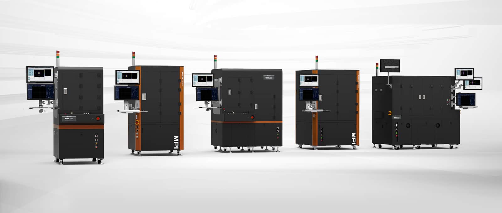
AVIOR Series Overview
The MPI AVIOR series offers a broad lineup of high performance prober systems targeting the Optical Communications market. Our prober systems are available in Top emitting (TP), Flip chip (FP) emitting and Die/Package (DP) configurations to meet your specific test requirements. Whether it be R&D or mass production, MPI has a solution that will meet your needs for accurate and reliable measurements in conjunction with a reduced cost-of-test.
MARKETS SERVED
Optical Com.
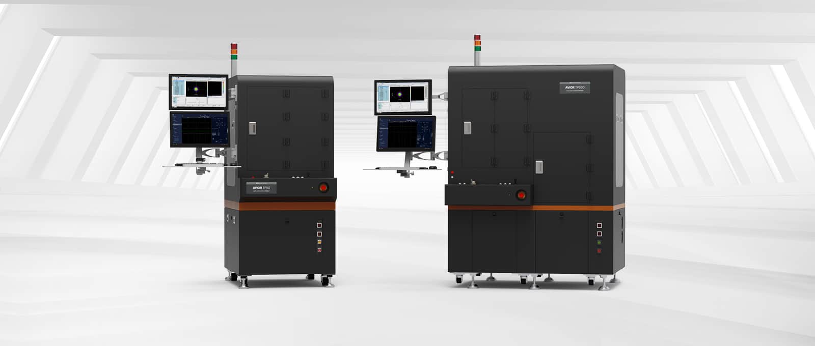
AVIOR Top Prober (TP) Series Key Features
- The highly configurable lineup of wafer probers handle 2” ~ 8” wafers, with a comprehensive selection of chuck systems and probing mechanisms to choose from.
- Highly accurate electrical and optical measurements (DC/RF/Pulsed).
- Selectable contact mechanism options include: Probe Card Holder (PCH), Wedge Probe Card and MPI F1 single probe module.
- Flexible choices of precision light collection and coupling optics to meet your specific test requirements.
- MPI prober control software provides comprehensive control functions from basic wafer alignment, mapping, probe mark inspection to the deployment of MPI’s advanced Needle Alignment Mechanism (NAM) technology.
- The MPI Photonics Test System features a user-centric design that can be flexibly configured and programmed according to your unique test requirements.
Flexibility: With support for multiple test recipes, the user can flexibly select or modify the workflow or edit parameters according to the product and tests being performed.
Production Management: Manage lab/production data via the intuitive and easy-to-use software interface. Integrated real-time system monitoring and reporting enable a smooth and fully unattended test process.
Seamless Integration: With MPI’s extensive instrument library, the MPI test system can easily interface with mainstream third-party measurement instruments to meet your unique testing needs.
CAPABILITY
Multiple Probing Mechanisms
Max. 8” Wafer Handling
CONFIGURATION
Semi Auto
Fully Auto
DUT
VCSEL
PD
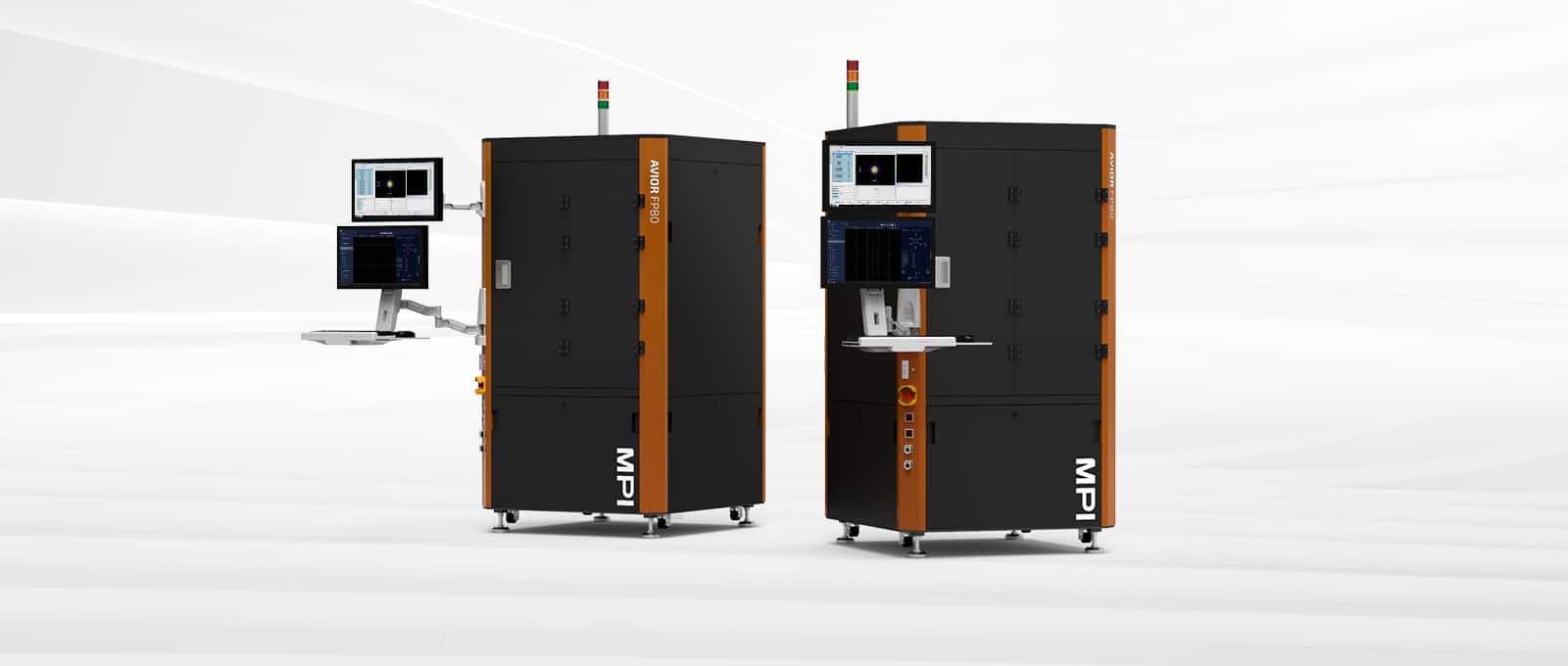
AVIOR Flip-chip Prober (FP) Series Key Features
- Multiple contact mechanism options include: Probe Card Holder, Wedge Probe Card and MPI F1 single probe module.
- Flexible choices of precision light collection and coupling optics to meet your specific test requirements.
- Comprehensive support for multiple probing schemes and optical input/output orientations:
- Wafer top-side electrical probe + bottom-side optical measurement
- Simultaneous probing of wafer top/bottom surfaces - MPI prober control software provides comprehensive control functions from basic wafer alignment, mapping, probe mark inspection to the deployment of MPI’s advanced Needle Alignment Mechanism (NAM) technology.
- The MPI Photonics Test System features a user-centric design that can be flexibly configured and programmed according to your unique test requirements.
Flexibility: With support for multiple test recipes, the user can flexibly select or modify the workflow or edit parameters according to the product and tests being performed.
Production Management: Manage lab/production data via the intuitive and easy-to-use software interface. Integrated real-time system monitoring and reporting enable a smooth and fully unattended test process.
Seamless Integration: With MPI’s extensive instrument library, the MPI test system can easily interface with mainstream third-party measurement instruments to meet your unique testing needs.
CAPABILITY
Multiple Probing Mechanisms
Max. 8” Wafer Handling
CONFIGURATION
Semi Auto
Fully Auto
DUT
VCSEL
PD
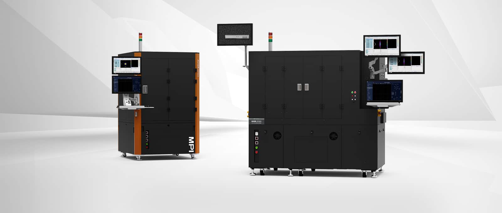
AVIOR Die Prober (DP) Series Key Features
- A wide range of configuration options perfectly designed for testing VCSELs, EELs, Packaged devices and more.
- Extremely fast probing and sorting cycle for reduced cost-of-test.
- Optimized material handling structure offers various input/output options.
- Supports a broad range of temperatures ranging from high temperature to sub-zero testing.
- Multiple test stations for mounting optical components for LIV, Near Field, and Far Field testing.
CAPABILITY
Multiple Probing Mechanisms
Max. 8” Wafer Handling
CONFIGURATION
Fully Auto
DUT
VCSEL
EEL
PD
More Information
Are you interested in this product and need further information?
please click below for a quick response or
Email us: ast-systems@mpi-corporation.com
Need help or have questions?