
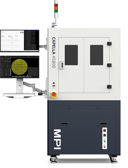
Automated Visual Inspection System
AS800 Series
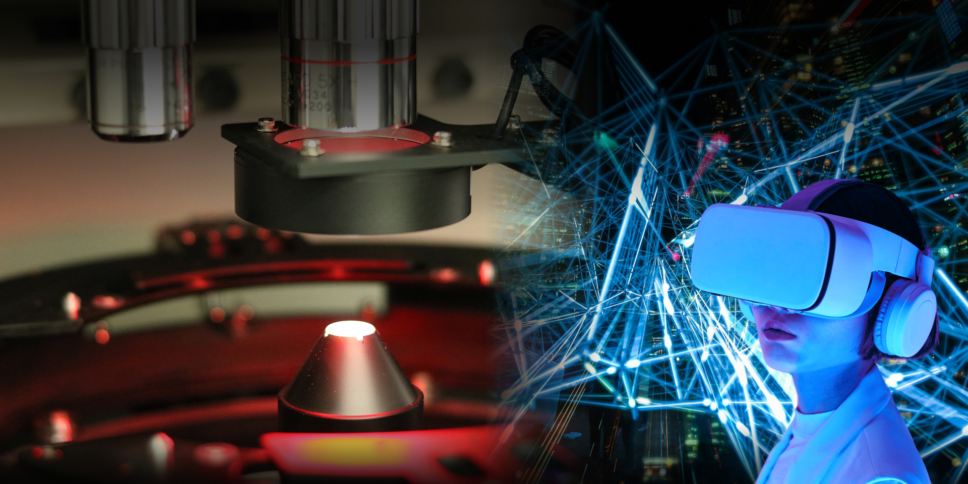

AS800 Overview
Advanced 2D Automated Visual Inspection
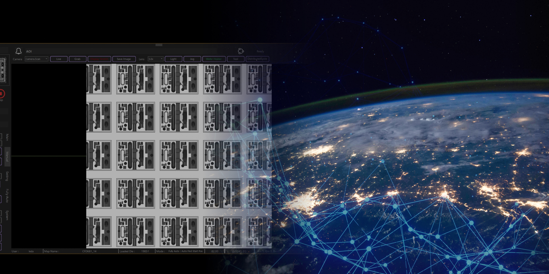
The AS800 is a cutting-edge 2D automated visual inspection (AVI) system engineered for high-precision and efficient defect detection in wafer manufacturing. Designed with modular architecture, adaptable lighting configurations, and AI-Driven recognition, it ensures superior quality control throughout the production process.
From wafer surface defect inspection and internal crack analysis to high-precision specialized applications, the AS800 delivers reliable, high-performance solutions that optimize yield and strengthen your competitive advantage.
Key Features

Adaptive Change Kit
Swiftly adapts to different wafer carrier sizes and shapes for seamless process integration.

Versatile Optical System
Turret-style optics enable automatic switching between 2.5x, 5x, and 10x magnifications for precise inspection.

High-Efficiency Docking Loader
Dual AVI stations ensure fast loading, unloading, and smooth multi-machine connectivity.

Modular Inspection Flexibility
Customizable 2D vision and contour inspection modules provide multi-functional capabilities.
Solutions
Solving Your Most Critical Inspection Challenge
Consistent Quality Assurance
The AS800 is engineered to eliminate inconsistencies in quality control by combining high-precision imaging with a flexible lighting system. Designed for a wide range of materials and structures, it reduces false positives and undetected defects, ensuring superior product reliability.
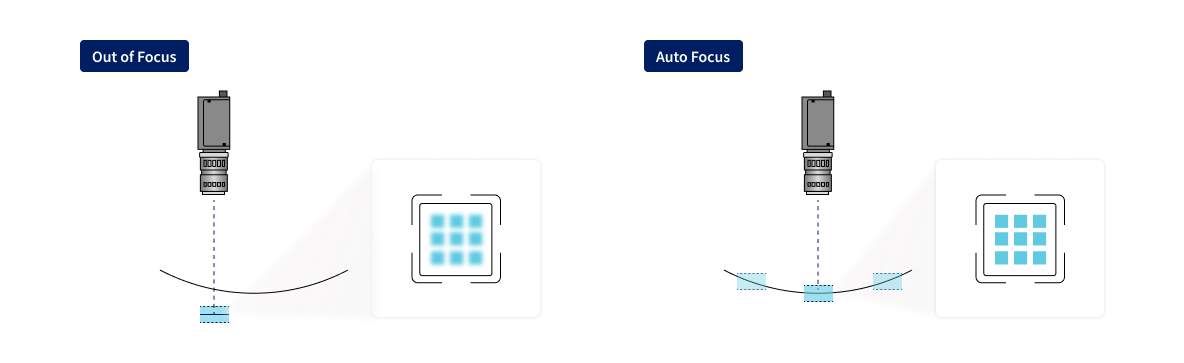
Advanced auto-focus technology guarantees sharp imaging, enhancing both inspection speed and accuracy.
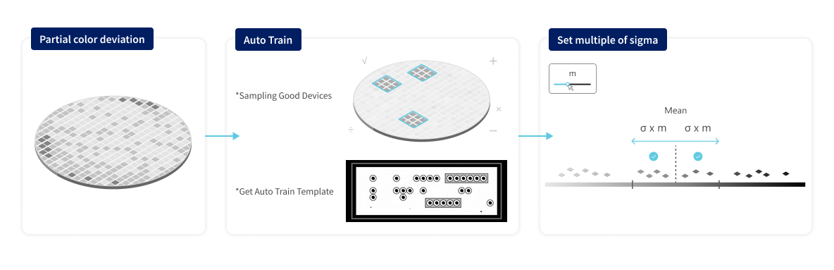
The Auto-Train Teaching function refines detection quality, minimizing false positives and missed defects.
High-penetration lighting enables non-destructive detection of internal cracks and microscopic defects, safeguarding production integrity.
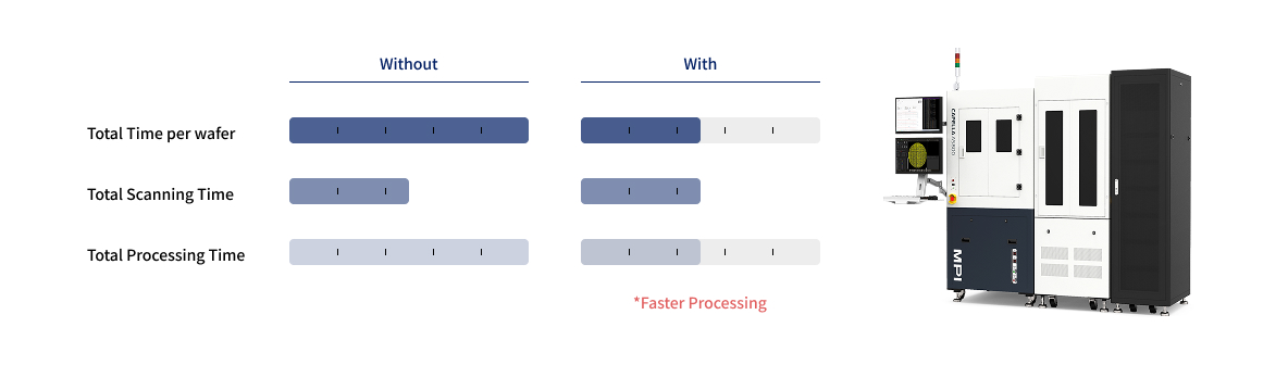
Maximizing Production Efficiency
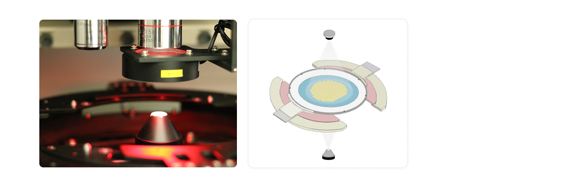
By integrating intelligent automation and real-time defect classification, the AS800 significantly reduces inspection time and manual intervention. Its dual-sided simultaneous inspection further accelerates throughput and optimizes operational efficiency.
Simultaneous front and back wafer analysis minimizes handling cycles, improving overall process automation.
Equipped with two high-speed distributed processing units, expandable to meet high-load inspection demands.
Lowering Operation Cost
With AI-powered defect recognition and automated verification, the AS800 reduces manual re-inspections while improving overall detection accuracy. It consolidates inspection data into a single, standardized report, reducing human intervention and error rates.
Automates defect identification and verification, reducing reliance on manual review.
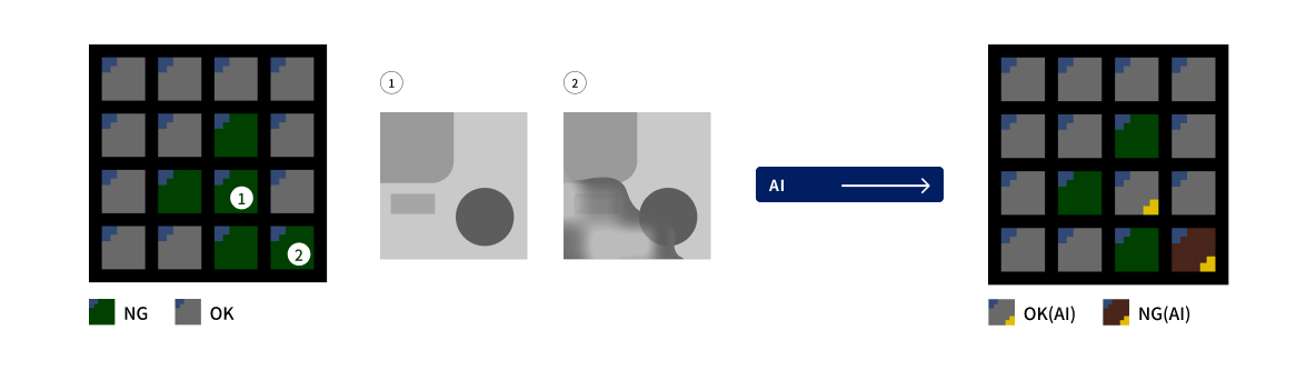
Automatically merges front, back, and multi-magnification results into a unified, error-free report.

 Wafer Warpage
Supports
± 3 mm
 Dual-Sided Inspection
Efficiency
↑ 50 %
 AI Driven Inspection
Accuracy
↑ 99 %
Applications
2D Inspection
High-precision front and back inspection.
Detects pad defects, peeling, chipping, and epitaxial defects.
3D Inspection
Comprehensive 3D measurement and surface profiling.
Optimized for complex structures, improving depth and accuracy.
Visible Light Inspection
Precisely detects surface structures.
Supports pad scratch detection, emission area defects, and other surface irregularities.
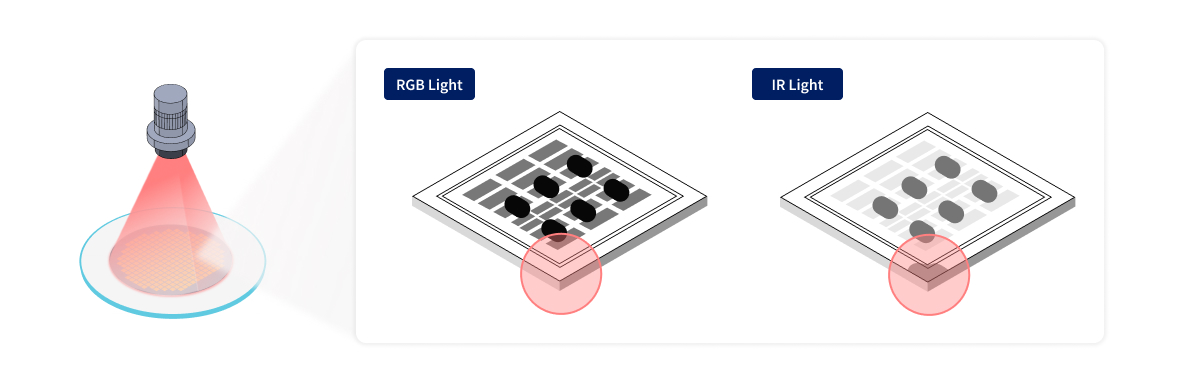
IR Light Inspection
High-penetration infrared for subsurface crack detection.
Enables non-destructive internal defect analysis with minimal thermal impact.
UV Light Inspection
Specialized for micro-crack detection, capturing fine surface defects.
Ensures structural integrity in Micro LED applications, enhancing stability and reliability.
Si (Silicon)
Essential for defect inspection in IC, MEMS, sensor, and memory manufacturing, ensuring high precision and reliability.
GaAs (Gallium Arsenide)
Widely used in optical communications (PD, VCSEL), LED, and RF applications, providing precise inspection to enhance component quality.
GaN (Gallium Nitride)
Optimized for high-frequency and high-power electronics, delivering accurate performance assessment of power amplifiers to ensure reliability and efficiency.
EEL (Edge-Emitting Laser)
Designed for optical communications (PD, VCSEL), industrial lasers, and medical devices, offering high-precision inspection to maintain component integrity and stability.
2D Inspection
High-precision front and back inspection.
Detects pad defects, peeling, chipping, and epitaxial defects.
3D Inspection
Comprehensive 3D measurement and surface profiling.
Optimized for complex structures, improving depth and accuracy.
Visible Light Inspection
Precisely detects surface structures.
Supports pad scratch detection, emission area defects, and other surface irregularities.
IR Light Inspection
High-penetration infrared for subsurface crack detection.
Enables non-destructive internal defect analysis with minimal thermal impact.
UV Light Inspection
Specialized for micro-crack detection, capturing fine surface defects.
Ensures structural integrity in Micro LED applications, enhancing stability and reliability.
Si (Silicon)
Essential for defect inspection in IC, MEMS, sensor, and memory manufacturing, ensuring high precision and reliability.
GaAs (Gallium Arsenide)
Widely used in optical communications (PD, VCSEL), LED, and RF applications, providing precise inspection to enhance component quality.
GaN (Gallium Nitride)
Optimized for high-frequency and high-power electronics, delivering accurate performance assessment of power amplifiers to ensure reliability and efficiency.
EEL (Edge-Emitting Laser)
Designed for optical communications (PD, VCSEL), industrial lasers, and medical devices, offering high-precision inspection to maintain component integrity and stability.
Technical Specs
Model Name
AS800
Inspection camera
25MP, 31MP Mono Color
Magnification / Resolution
2.5x 1.38µm/pixel
5x 0.69µm/pixel
10x 0.345µm/pixel
Max. Wafer Handling Size
8”
Distributed Computing Units
Standard: 2 units
Optional: up to 6 units
Vibration control standards
VC-D level
Dual-Sided Inspection
Color Variation Defect Detection
Quick Carrier Exchange
Wafer Warpage Compensation
Features Demo
More Products


